Phase adjustment apparatus and semiconductor test apparatus

a phase adjustment and test apparatus technology, applied in the direction of semiconductor/solid-state device testing/measurement, pulse technique, instruments, etc., can solve the problems of jitter or waveform distortion, difficult to match all the lengths of the pattern wiring of thousands of transmission signals, and take time for adjustment work to adjust the fixed delay device, etc., to achieve stable and optimal timing

Inactive Publication Date: 2008-02-26
ADVANTEST CORP
View PDF9 Cites 4 Cited by
  • Summary
  • Abstract
  • Description
  • Claims
  • Application Information

AI Technical Summary

Benefits of technology

[0025]Accordingly, it is an object of the present invention to provide a phase adjustment apparatus and a semiconductor test apparatus for automatically correcting irregularities of propagation delay of a transmission signal transmitted between apparatuses while synchronized with a high-speed clock, so that the transmission signal can be received at stable and optimal timing in a receiving end.
[0026]In addition, it is an object of the present invention to provide a phase adjustment apparatus and a semiconductor test apparatus for automatically correcting irregularities of propagation delay of a transmission signal, so that the transmission signal can be received at stable and optimal timing in a receiving end, even if the phase relation between the transmission signal received and a clock of the receiving end in which retiming is performed on the signal is in the unknown state.
[0027]In addition, it is an object of the present invention to provide a phase adjustment apparatus and a semiconductor test apparatus for automatically correcting irregularities of propagation delay at the time of present operation, so that the retiming state which was most stable can be maintained under the present power supply voltage condition and the surrounding temperature condition in the operation state with a power source being supplied.
[0028]In addition, it is an object of the present invention to provide a phase adjustment apparatus and a semiconductor test apparatus for automatically correcting the phase relation of retiming, so that the signal can be received at stable and optimal timing, even in case of changing the period of a clock.
[0031]According to this invention, it is possible to realize a phase adjustment apparatus and a semiconductor test apparatus for automatically correcting irregularities of propagation delay of a transmission signal transmitted between apparatuses while synchronized with a high-speed clock, so that the transmission signal can be received at stable and optimal timing in a receiving end.

Problems solved by technology

It is practically difficult to match all of the lengths of the pattern wirings of thousands of transmission signals which connect both the LSIs or the amounts of the propagation delay.
And there is also jitter or waveform distortion caused by the reflection of the transmission signal.
In addition, there is a difficulty that it takes time for adjustment work to adjust the fixed delay device of a desired delay amount while selecting it.
And there is also a difficulty that in response to tens or hundreds of transmission signals, an area is needed to mount a lot of the delay devices 80 on a board, so the mounting density of the board decreases.
If it changes, there is a problem that the retiming operation in accordance with this becomes unstable.
In addition, if the timing condition under which retiming is performed on the transmission signal 20s changes due to the board replacement, there might occur some of lots of transmission signals which are not necessarily in the stable timing state.
And there is also manufacture irregularity in an IC or LSI itself or irregularity of propagation delay according to the difference of makers, whereby the timing does not always be in the optimal retiming state.
According to this, if a high-speed clock whose operation margin is narrow is applied, there is a possibility that a malfunction is occasionally caused unless the optimal phase condition is set.
And in case of changing the period of a clock, the phase relation between the transmission signal received and the clock of the receiving end in which retiming is performed on the signal does not be in the optimal phase condition.
In operation with the power source being supplied, it is often uncertain whether the apparatus is operating while maintaining the retiming state which was stable under the present power supply voltage condition and the surrounding temperature condition or not.
In terms of that point, the conventional art has a practical problem which is not desirable.

Method used


Image

  • Phase adjustment apparatus and semiconductor test apparatus
  • Phase adjustment apparatus and semiconductor test apparatus
  • Phase adjustment apparatus and semiconductor test apparatus

Examples


Embodiment Construction

[0075]The invention will now be described based on the preferred embodiments, which do not intend to limit the scope of the present invention, but exemplify the invention. All of the features and the combinations thereof described in the embodiment are not necessarily essential to the invention.

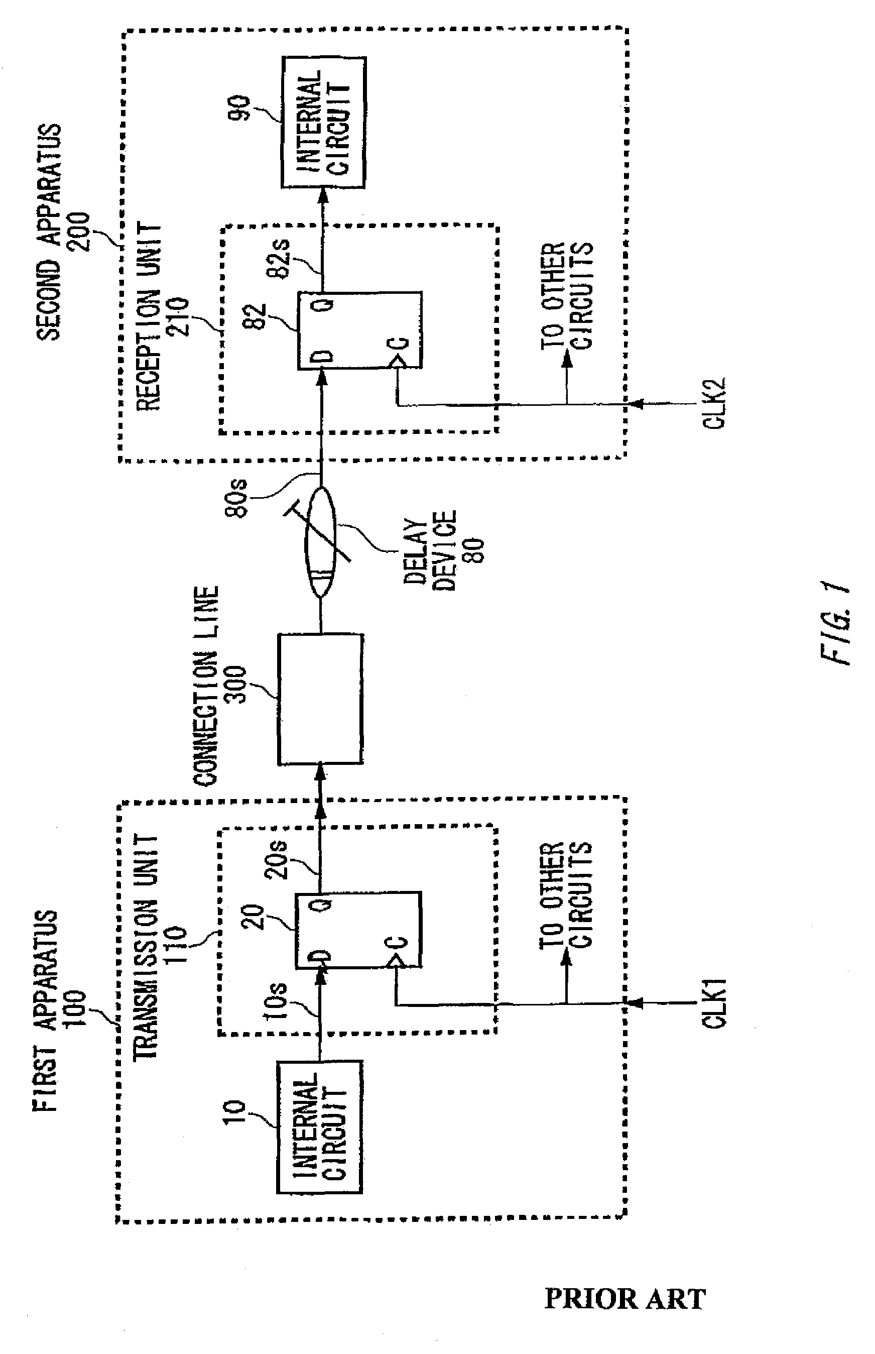
[0076]The present invention will hereafter be described referring to FIGS. 2 and 3. Further, elements in response to the conventional configuration are given the same symbols, and matters repeated will not be described.

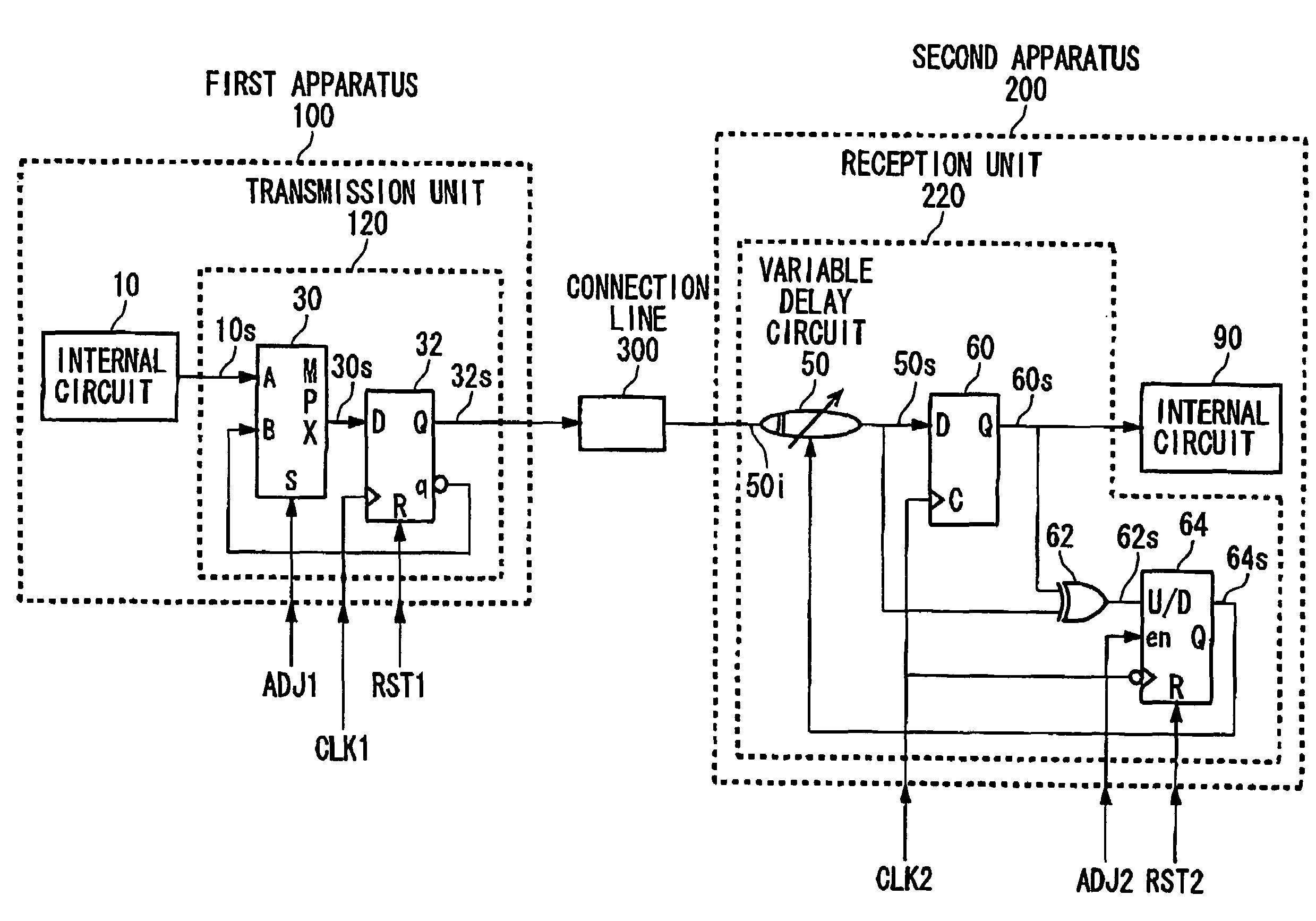
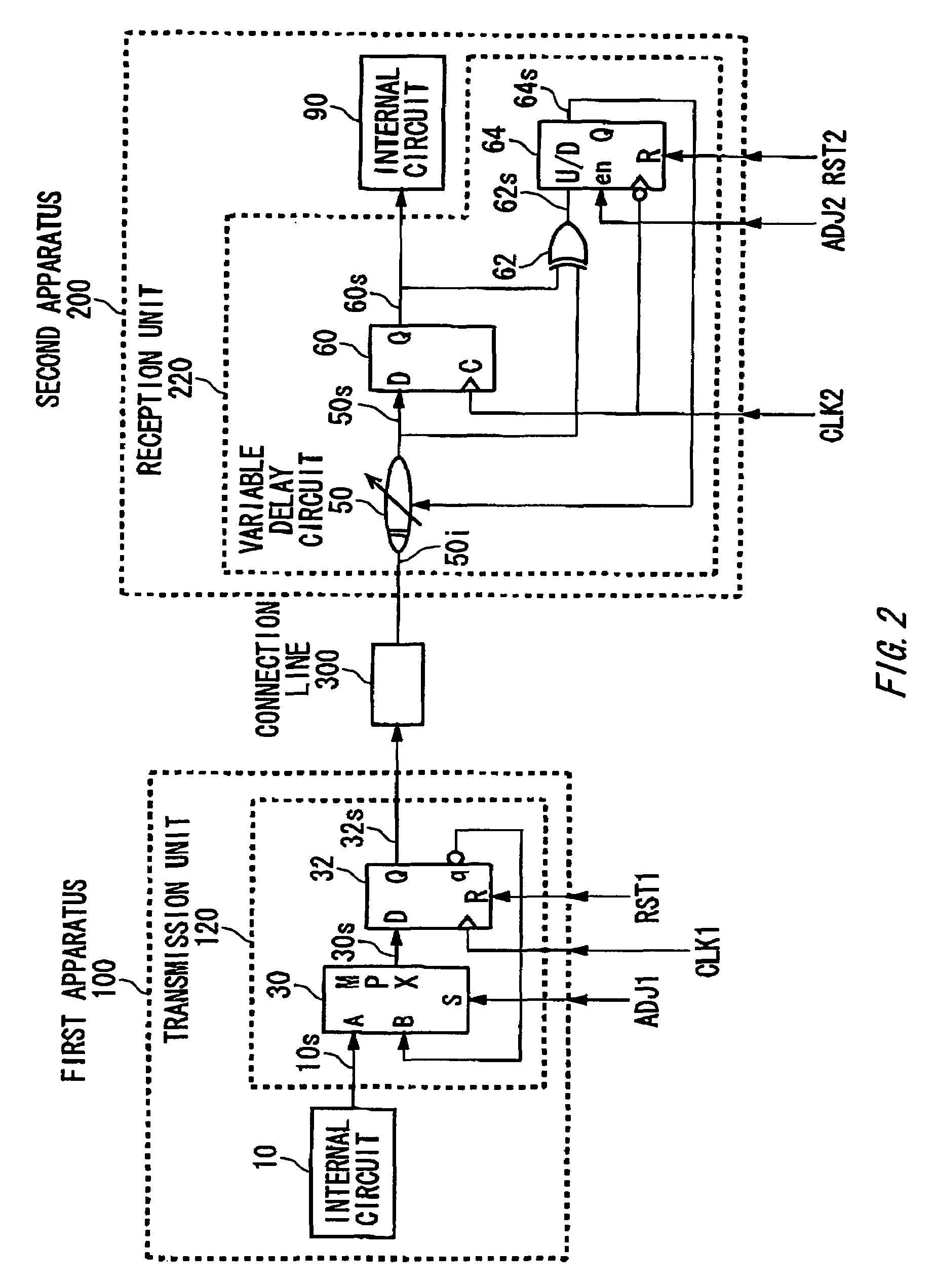
[0077]FIG. 2 shows a configuration example of a phase adjustment apparatus of a transmission signal for performing a phase adjustment of timing for a clock according to this invention. It is herein simply assumed that one transmission signal is received and retiming is performed on the signal with a clock.

[0078]These main configuration elements include a first clock CLK1, a second clock CLK2, adjustment mode signals ADJ1 and ADJ2, reset signals RST1 and RST2, a first apparatus ...


PUM


Abstract

A phase adjustment apparatus and a semiconductor test apparatus for automatically correcting irregularities of propagation delay of a transmission signal, so that the transmission signal transmitted between apparatuses while synchronized with a high-speed clock can be received at a stable optimal timing at a receiving end. The phase adjustment apparatus for transmitting a transmission signal synchronized with a clock between a first apparatus of the sending end and a second apparatus of the receiving end includes phase adjustment means used when retiming the transmission signal with the clock of the receiving end of the second apparatus. That is, the phase adjustment means corrects an unknown phase relationship between the clock of the receiving end and the transmission signal and delays the transmission signal by a specified amount for adjustment so that the signal can be received with a stable retiming condition.

Description

[0001]The present application is a continuation application of PCT / JP02 / 12121 filed on Nov. 20, 2002 which claims priority from Japanese patent application No. 2001-354222 filed on Nov. 20, 2001, the entire contents of which are incorporated herein by reference for all purposes.BACKGROUND OF THE INVENTION[0002]1. Field of the Invention[0003]The present invention relates to a phase adjustment apparatus of a transmission signal transmitted between apparatuses while synchronized with a clock and a semiconductor test apparatus using the phase adjustment apparatus. More particularly, the present invention relates to a phase adjustment apparatus and a semiconductor test apparatus for automatically correcting irregularities of propagation delay of a transmission signal transmitted between apparatuses while synchronized with a high-speed clock, so that the transmission signal can be received at stable and optimal timing in a receiving end.[0004]2. Related Art[0005]FIG. 6 shows the represent...

Claims


Application Information

Patent Timeline
Patent Type & Authority Patents(United States)
IPC IPC(8): H03H7/30G01R31/319H03K5/135H04L7/033
CPCG01R31/31922H03K5/135H04L7/0037H04L7/0331H04L7/0041G01R31/26H01L22/00H04L7/00
Inventor GOISHI, MASARU
Owner ADVANTEST CORP
Why Eureka
Try Eureka