SMD chip handling apparatus

a technology for smd chips and handling apparatuses, which is applied in the direction of gas flame welding apparatus, soldering auxiliaries, printed circuit aspects, etc., can solve the problems of difficult and awkward to fetch and place smd chips, the smd chip would readily pop out of the tweezers, and the care must be exercised in picking up smd chips with the tweezers, etc., to achieve cost-effectiveness, simple structure, and easy operation

Inactive Publication Date: 2008-03-04
WONG CHI MING +1
View PDF8 Cites 4 Cited by
  • Summary
  • Abstract
  • Description
  • Claims
  • Application Information

AI Technical Summary

Benefits of technology

[0006]It is therefore an object of the present invention to provide an apparatus for fetching an SMD chip effectively.
[0007]It is another object of the present invention to provide a portable apparatus operative manually for fetching and positioning an SMD chip on a printed circuit board with ease.
[0010]It is yet another object of the present invention to provide a portable manually operative apparatus for retaining an SMD chip safely in place for de-soldering it from a printed circuit board and removing it therefrom.
[0011]It is still another object of the present invention to provide a manually operative apparatus which is simple in structure and easy to operate.
[0012]It is still another object of the present invention to provide a manually operative portable apparatus which is cost effective for hobbyists and an individual circuit developers to acquire.

Problems solved by technology

Heretofore, it has been problematic for an electronic hobbyist and circuit developer in handling and soldering a surface mounted device, commonly referred to as an SMD chip, on a printed circuit board in fabricating a prototype electronic circuit.
With such extremely small physical dimensions, it is very difficult and awkward to fetch and to place the SMD chip at a selected position on the printed circuit board, and maintaining it in position while soldering it onto the board.
Firstly, considerable care must be exercised in picking up an SMD chip with the tweezers, as the chip would fall off the tweezers if an insufficient clamping force is applied; on the other hand, the SMD chip would readily pop out from the tweezers if too much force is applied.
Furthermore, the manual operation of maintaining the chip in place with the tweezers or other holding means during soldering, is also extremely difficult to carry out since the tweezers or holding means must be held in place, while having simultaneously to feed solder with a solder wire to the chip and to apply heat to the solder with a soldering iron.
However, such devices are very complex in construction, and are still difficult to operate; and moreover they are far too expensive to acquire by a hobbyist or an individual electronic circuit developer for making prototype electronic circuits.

Method used


Image

  • SMD chip handling apparatus
  • SMD chip handling apparatus
  • SMD chip handling apparatus

Examples


Embodiment Construction

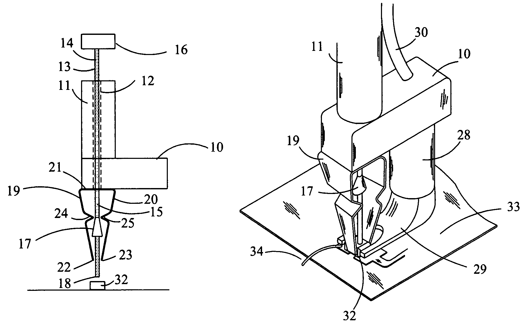
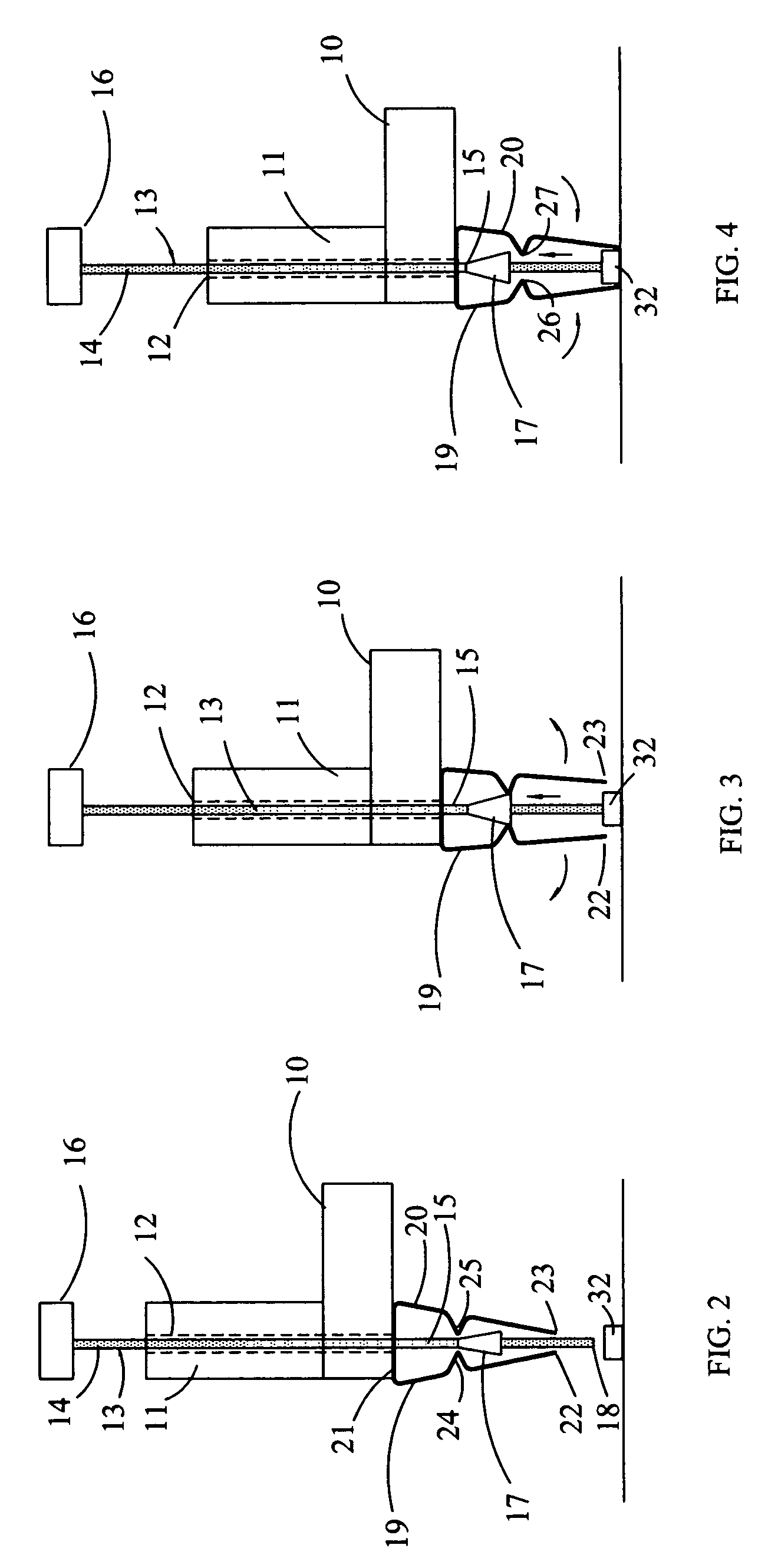
[0021]With reference to the accompanying drawings wherein like reference numerals designate corresponding parts in the several views, the apparatus according to the present invention has a main body 10 which may be rectangular in shape as shown. An elongated tubular housing 11 extends vertically upwards from a front portion of the main body 10. In the exemplary embodiment shown, the tubular housing 11 is preferably cylindrical in shape. The tubular housing 11 may be mounted to or integrally formed with the main body 10 by molding. A vertical through channel opening 12 is formed in the tubular housing 11 and the front portion of the main body 10 directly below the tubular housing 11. An elongated rod 13 is slidably mounted within the channel opening 12. An upper portion 14 of the rod 13 extends above the upper end of the tubular housing 11 and its lower end portion 15 extends beyond the lower edge of the main body 10. A button 16 is mounted on the upper end of the rod 13 such that th...


PUM

PropertyMeasurementUnit
heightaaaaaaaaaa
heightaaaaaaaaaa
heightaaaaaaaaaa

Abstract

The apparatus is for securely fetching and positioning an SMD chip on a printed circuit board and soldering the same to the board. Two spring plates form the clasping fingers which are wedged apart to a width larger than the width of the SMD chip by an expander formed on an elongated rod slidably mounted within a vertical tubular housing. An SMD chip may be safely fetched by pressing the rod on the top of the SMD with a continuous depressing motion until the fingers clasp the SMD chip safely therebetween. A soldering unit with a bifurcate soldering head located juxtaposed to the fingers is operative to solder the SMD chip to the printed circuit board while the SMD chip is safely held in place.

Description

BACKGROUND OF THE INVENTION[0001]1. Field of the Invention[0002]This invention relates to an apparatus for holding and soldering a miniature size chip component on a printed circuit board and more particularly relates to a portable device for facilitating electronic hobbyists and circuit developers in surface mounting and soldering a miniature SMD chip component on a printed circuit board or de-soldering it therefrom.[0003]2. Background Art[0004]Heretofore, it has been problematic for an electronic hobbyist and circuit developer in handling and soldering a surface mounted device, commonly referred to as an SMD chip, on a printed circuit board in fabricating a prototype electronic circuit. Generally, an SMD chip has the physical dimensions of 0.12 inch by 0.06 inch or 0.08 inch by 0.05 inch or 0.04 inch by 0.02 inch, and a height of about 0.025 inch. With such extremely small physical dimensions, it is very difficult and awkward to fetch and to place the SMD chip at a selected positi...

Claims


Application Information

Patent Timeline
Patent Type & Authority Patents(United States)
IPC IPC(8): B23P19/00
CPCB23K3/087H05K3/3442H05K13/0404H05K13/0465B23K2201/40H05K3/3494Y10T29/4913H05K2203/0195Y10T29/53196Y10T29/53178Y10T29/53174Y10T29/53183Y10T29/49144H05K2201/10636B23K2101/40H05K13/0447H05K13/0491Y02P70/50
Inventor WONG, CHI MINGCHAN, WOON-WAI
Owner WONG CHI MING
Why Eureka
Try Eureka