Hole plugging method for printed circuit boards, and hole plugging device

a printed circuit board and hole plugging technology, which is applied in the direction of printed element electric connection formation, non-printed mask formation, conductive pattern formation, etc., can solve the problem of surface circuit pattern, difficult abrasive process to expose surface circuit pattern, and limit the densification degree of the board, etc. problem, to achieve the effect of smooth plugging of solder resist insulating material

Inactive Publication Date: 2008-03-04
LG INNOTEK CO LTD
View PDF18 Cites 1 Cited by
  • Summary
  • Abstract
  • Description
  • Claims
  • Application Information

AI Technical Summary

Benefits of technology

[0024]Therefore, an object of the present invention is to provide a hole plugging method for printed circuit boards and a hole plugging device in accordance therewith, capable of smoothly plugging a solder resist insulating material in a via hole formed to electrically connect a circuit pattern formed on the surface of the board and a circuit pattern formed in the board, or in a through hole formed to electrically connect the circuit patterns on the both side surfaces of the board.
[0025]Another object of the present invention is to provide a hole plugging method for printed circuit boards and a hole plugging device in accordance therewith capable of plugging a resin insulating material by coating the resin in spaces between the circuit patterns just to the height of the circuit patterns and at the same time, minimizing the amount of insulating material coated on the circuit pattern.
[0026]Still another object of the present invention is to provide a hole plugging method for printed circuit boards and a hole plugging device in accordance therewith capable of preventing bubbles from remaining behind in the insulating material plugged in the spaces between via holes, through holes or circuit patterns on the board.
[0027]Still another object of the invention is to provide a hole plugging method for printed circuit boards and a hole plugging device in accordance therewith capable of preventing an integrated circuit on the board from being damaged by restraining the formation of residual bubbles in the insulating material in the spaces between the via holes, through holes or circuit patterns on the board sufficiently.

Problems solved by technology

However, the interval between the through holes 1d can not be narrowed beyond a certain spacing and there is thus a limitation in the densification degree of the board when the sizes of tools and avoidance of damage to the board 1 in the processing are taken into consideration.
However, removing the solder resist SR afterwards by an abrasive process to expose the surface circuit pattern 1a is not easy since the solder resist SR is coated covering the surface circuit pattern 1a completely and damages may result to the surface circuit pattern 1a in case of removing the solder resist SR by using a brush and the like.
Air bubbles remaining behind in the solder resist SR are discharged due to the high heat when the integrated circuit (not shown) is mounted, and accordingly the circumferential circuit patterns, solder resist and integrated circuit can be damaged even though the solder resist SR is filled in the via hole 1c and the through hole 1d.
Also, the coefficients of thermal expansion of the integrated circuit and the board are different and accordingly, the board can be damaged when high heat is generated in the integrated circuit.
However, there are disadvantages in the cost and the manufacturing time, in that a vacuum device must be equipped and repeated operation of exposure under the vacuum condition and plugging operations are needed thus to reduce productivity.

Method used


Image

  • Hole plugging method for printed circuit boards, and hole plugging device
  • Hole plugging method for printed circuit boards, and hole plugging device
  • Hole plugging method for printed circuit boards, and hole plugging device

Examples


Embodiment Construction

[0048]Reference will now be made in detail to the preferred embodiments of the present invention, examples of which are illustrated in the accompanying drawings.

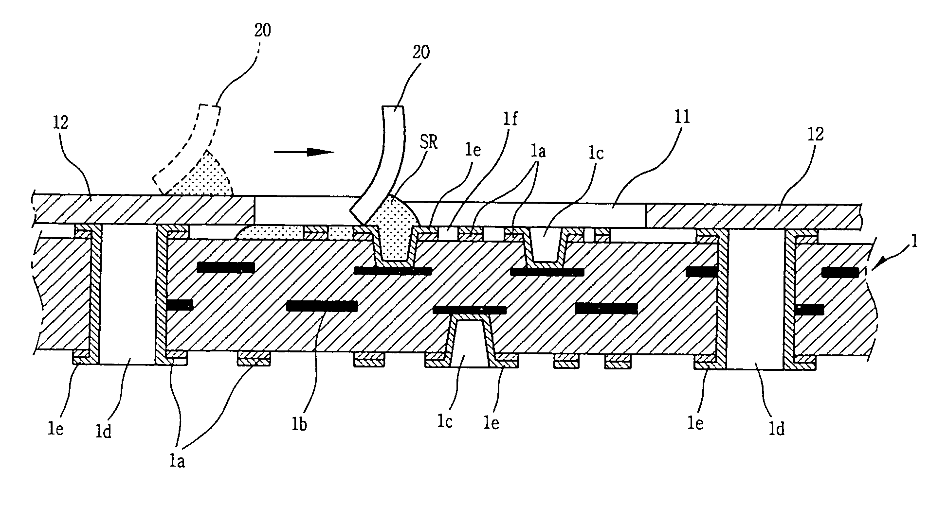
[0049]FIG. 3 is a perspective view showing a hole plugging device for printed circuit boards according to an embodiment of the present invention, FIG. 4 is a cross-sectional view showing the hole plugging device and method for printed circuit boards according to the embodiment of the present invention and FIG. 5 is a detail view showing a state where a hole is plugged in a printed circuit board according to the embodiment of the present invention.

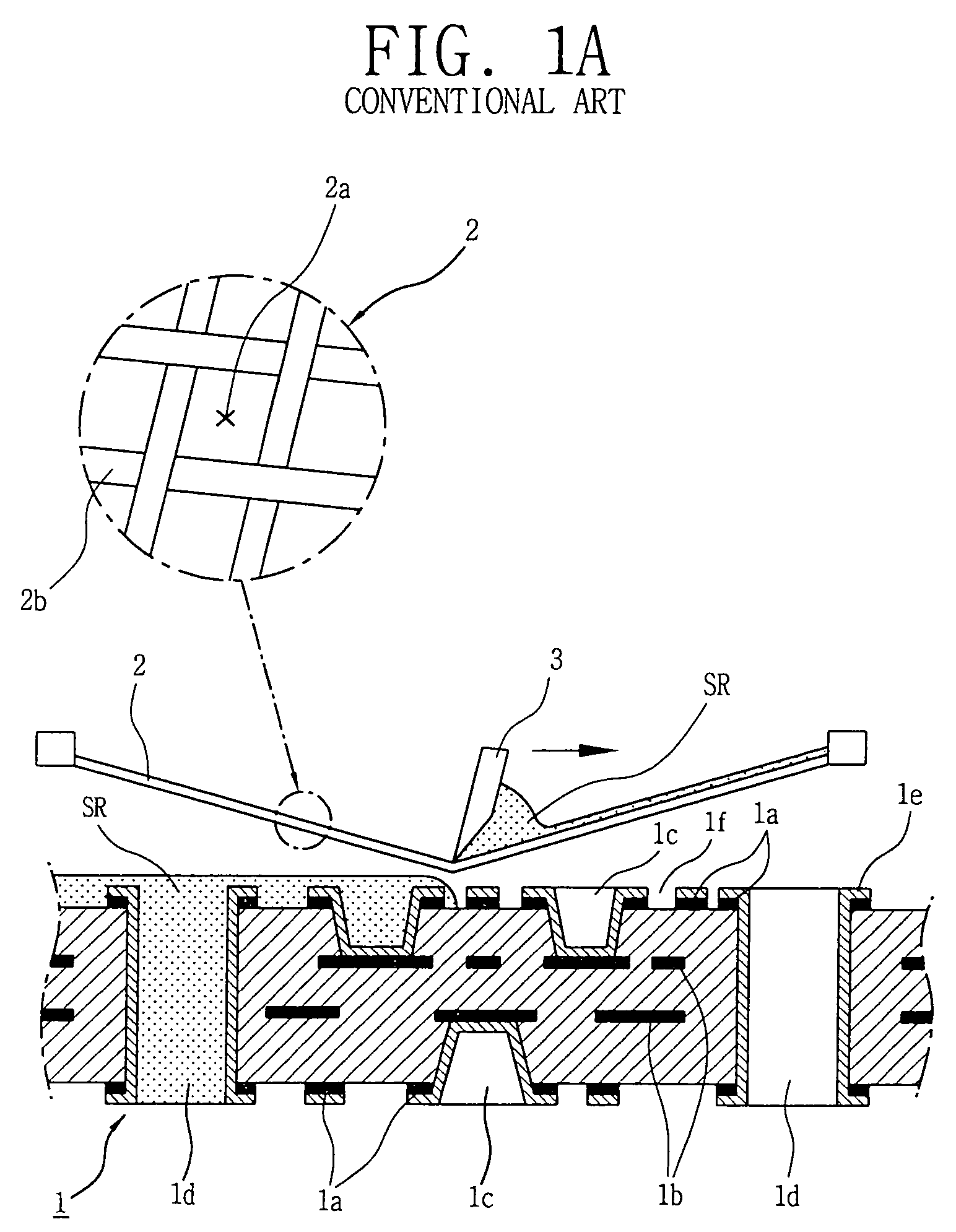
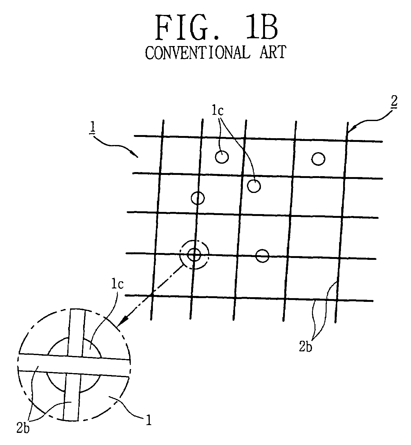
[0050]Firstly, the printed circuit board includes a surface circuit pattern 1a and internal circuit conductors 1b are formed on and in a board 1 respectively, a via hole 1c formed to electrically connect the surface circuit pattern 1a and the internal circuit pattern 1b by a conductive layer 1e, and a through hole 1d formed to connect the both side surface circuit patterns 1a by the...


PUM

PropertyMeasurementUnit
diameteraaaaaaaaaa
diameteraaaaaaaaaa
diameteraaaaaaaaaa

Abstract

A hole plugging method for a printed circuit board, a hole plugging device in accordance therewith and a manufacturing method in accordance therewith where a mask for selectively exposing a via hole, a through hole and a surface pattern of the printed circuit board is positioned on the board having the via hole and the through hole to electrically connect circuit patterns formed on the surface of the board and in the board and an insulating material is plugged in the via hole by abutting and pushing the material on the surface of the board. Therefore, the insulating material can be plugged smoothly without a void, the processing is simplified by plugging the insulating material just to the height of the circuit pattern in a space between the circuit patterns and accordingly, damage to the circuit pattern can be prevented.

Description

[0001]The present application is a divisional of U.S. patent application Ser. No. 10 / 043,146 filed on Jan. 14, 2002 now U.S. Pat. No. 6,954,985 for which priority is claimed under 35 U.S.C. § 120. This application also claims priority under 35 U.S.C. § 119(a) on Patent Application No. 31752 / 2001 filed in Korea on Jun. 7, 2001 and Patent Application No. 51853 / 2001 filed in Korea on Aug. 27, 2001. The entire contents of each of these applications are herein fully incorporated by reference.BACKGROUND OF THE INVENTION[0002]1. Field of the Invention[0003]The present invention relates to a hole plugging method for printed circuit boards, a hole plugging device which carries out such method and a manufacturing method in accordance, and particularly, to a hole plugging method for printed circuit board and to a hole plugging device and a manufacturing method in accordance therewith which plugs holes in a printed circuit board with an insulating resin or solder resist by abutting a squeegee o...

Claims


Application Information

Patent Timeline
Patent Type & Authority Patents(United States)
IPC IPC(8): H01R43/00H05K3/00H05K3/28H05K3/12H05K3/42H05K3/46
CPCH05K3/0094Y10T29/49144H05K3/28H05K2201/09509H05K2201/0959H05K2201/09881H05K2203/0278H05K2203/0557Y10T29/49155Y10T29/49135Y10T29/49126Y10T29/49128Y10T29/49117Y10T29/49124Y10T29/49165Y10T29/49167H05K3/1225
Inventor LEE, SUNG GUECHO, SUNG SIKKIM, YONG ILJANG, YONG SOONCHOI, HO SUNGKONG, SANG JINKIM, YOUNG HWAN
Owner LG INNOTEK CO LTD
Why Eureka
Try Eureka