
Color electroluminescence display device

a display device and color electroluminescence technology, applied in the direction of luminescence screens, discharge tubes, identification means, etc., can solve the problems of color purity deterioration and further pronounced disadvantage, and achieve the effect of preventing color mixture among adjoining pixels, efficient arrangement, and efficient arrangemen

Inactive Publication Date: 2008-03-04
SANYO ELECTRIC CO LTD
View PDF48 Cites 18 Cited by
  • Summary
  • Abstract
  • Description
  • Claims
  • Application Information

AI Technical Summary

Benefits of technology

[0018]In accordance with one aspect of the present invention, a first thin film transistor is disposed in a region between a gate line and a capacitor, and a second thin film transistor is disposed in a region between the capacitor and an EL element. This configuration allows the capacitor, the first thin film transistor, and the second thin film transistors to be densely arranged, thereby facilitating formation of a highly integrated configuration.
[0020]In accordance with still another aspect of the present invention, the capacitor includes a dent region in which the first thin film transistor is disposed. Thus, an efficient arrangement can be achieved.
[0021]In accordance with still another aspect of the present invention, the EL element includes a dent region in which the second thin film transistor is disposed. Thus, an efficient arrangement can be achieved.
[0022]In accordance with further aspect of the present invention, the capacitor and the EL element are disposed so as to adjoin each other in the column direction, such that space is provided in the vertical direction. Therefore, when forming a pixel electrode (for example, an anode), color mixture among adjoining pixels can be prevented, when metal mask positioning accuracy is low, thereby maintaining preferable color purity for even highly detailed displays.

Problems solved by technology

Because of such diffusion phenomenon or because of imperfect construction of the metal mask itself, colors in adjoining pixels are adversely mixed causing color purity to deteriorate.
Particularly in delta arrangements, wherein adjoining pixels in the column and row directions differ from one another, this disadvantage is further pronounced.

Method used


Image

  • Color electroluminescence display device
  • Color electroluminescence display device
  • Color electroluminescence display device

Examples


first embodiment

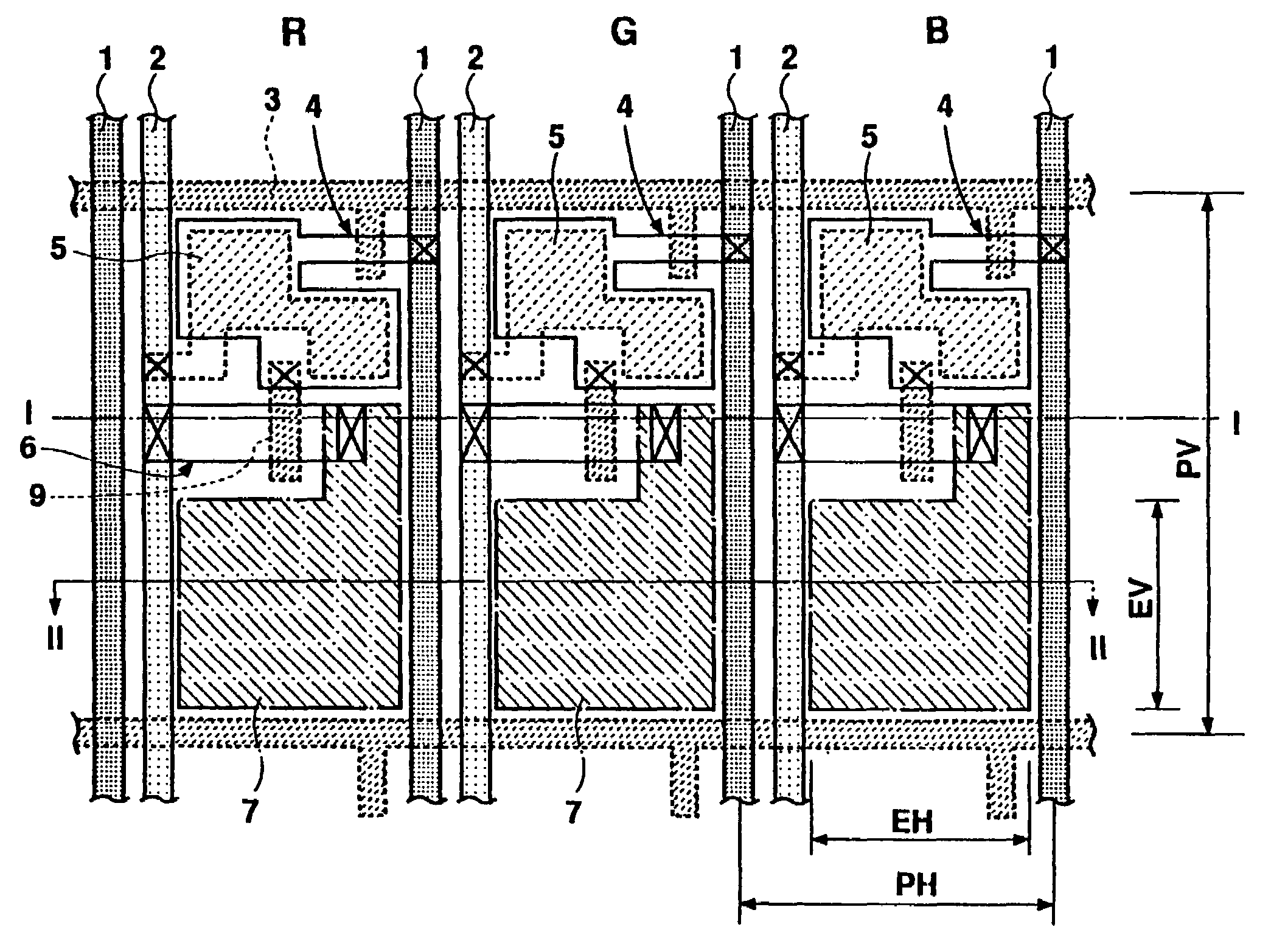
[0031]FIG. 5 is a plan view showing a color EL display device in accordance with the present invention, and depicts the configuration corresponding to three pixels of RGB. Further, FIG. 6A is a cross section taken along a line I-I of FIG. 5, and FIG. 6B is a cross section taken along a line II-II of FIG. 5. This embodiment exemplifies a configuration for the stripe pixel arrangement shown in FIG. 4A.

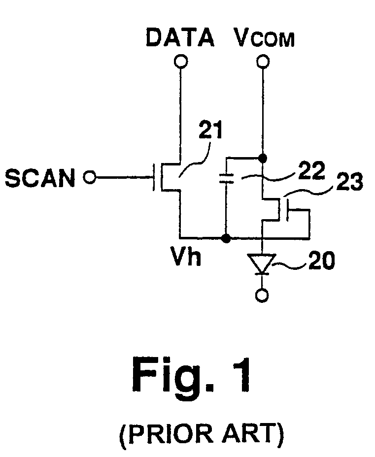
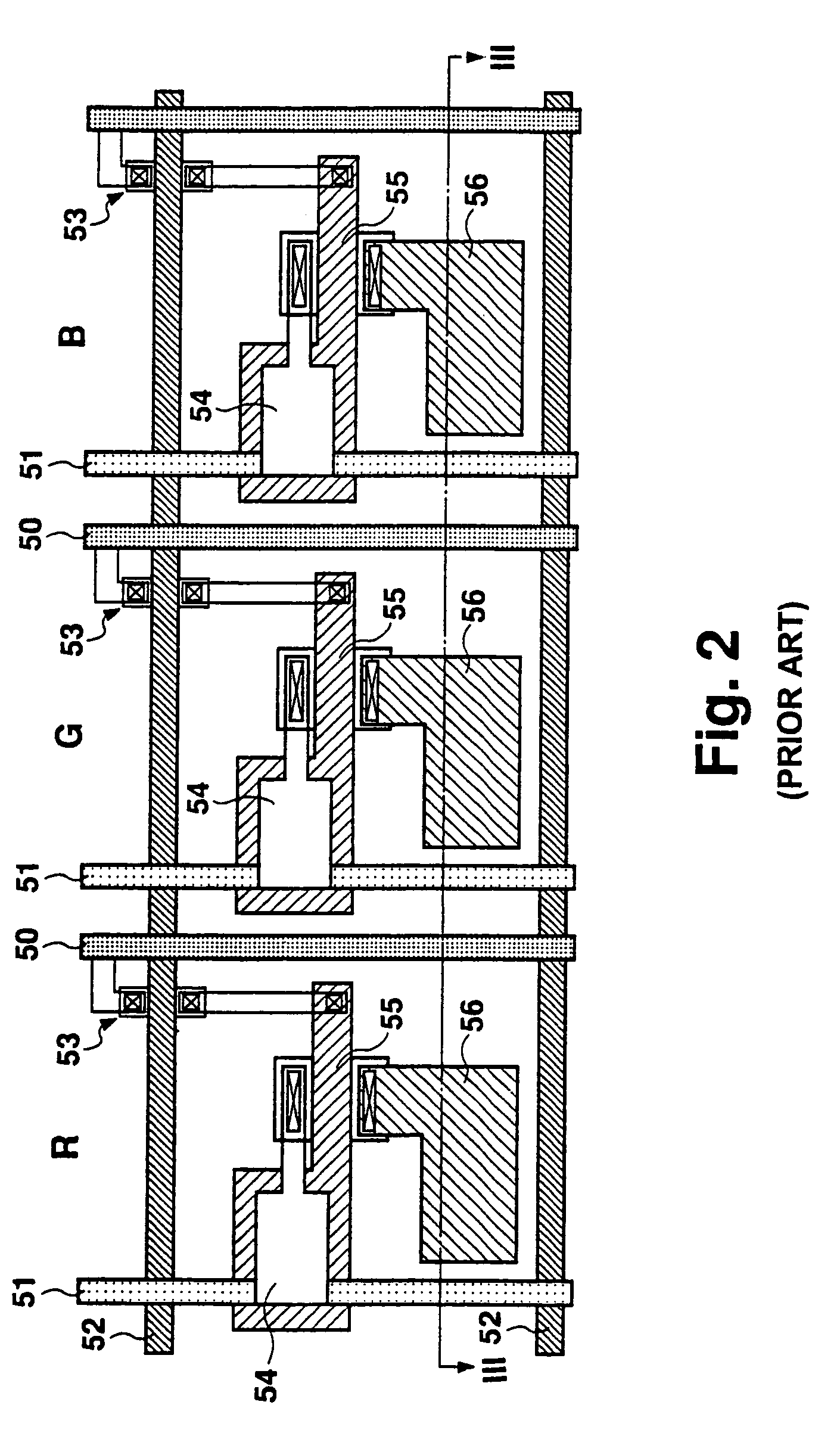
[0032]A driving circuit for each pixel in this embodiment is the same as that in FIG. 1, and the configuration of the device differs from the example shown in FIGS. 2 and 3 in the pattern arrangement and the cross section.

[0033]Referring to FIGS. 5, 6A and 6B, the device comprises a data line 1 made of aluminum for supplying a display signal DATA, a power supply line 2 made of aluminum for supplying a power from a drive source COM, and a gate line made of chrome for supplying a scan signal SCAN. Each pixel of the EL display further comprises a first TFT 4 corresponding to the first TFT 2...

second embodiment

[0039]FIG. 7 depicts, in plan view, the present invention. In FIG. 7, the same elements as shown in FIGS. 1, 5 and 6 are designated by the same reference numerals, and the detailed description thereof will be omitted. In FIG. 7, numeral 4 denotes a first TFT corresponding to the first TFT 21 of FIG. 1, numeral 5 denotes a capacitor corresponding to the capacitor 22 of FIG. 1, numeral 6 denotes a second TFT corresponding to the second TFT 23 of FIG. 1 and numeral 7 denotes an anode of the EL element 20 comprising ITO and constituting a pixel electrode. This embodiment exemplifies a configuration in the case of a delta pixel arrangement as shown in FIG. 4C.

[0040]In this embodiment, as in the first embodiment, the first TFT 4 is disposed in a region between the gate line 3 and the capacitor 5, and the capacitor 5 includes a dent region in which the first TFT 4 is disposed. Further, the second TFT 6 is disposed in a region between the capacitor 5 and the anode 7, and the anode 7 include...


PUM


Abstract

An electroluminescence display device is provided in which a plurality of pixels are arranged in row and column directions, including: a gate line extending in the row direction; a first thin film transistor whose gate is connected to the gate line; a drain line extending in the column direction; a capacitor connected to the drain line via the first thin film transistor; a second thin film transistor whose control electrode is connected to the capacitor; and an EL element connected to a supply line via the second thin film transistor and having a luminescent layer between an anode and a cathode. The first thin film transistor is disposed in a region between the gate line and the capacitor.

Description

CROSS-REFERENCE TO RELATED APPLICATION[0001]This application is a division of U.S. patent application Ser. No. 10 / 132,546, filed Apr. 25, 2002 now U.S. Pat. No. 6,690,118, the entire contents of which are incorporated herein by reference, which is a continuation of U.S. patent application Ser. No. 09 / 451,453, filed Nov. 30, 1999 now U.S. Pat. No. 6,429,599, the entire contents of which are incorporated herein by reference.BACKGROUND OF THE INVENTION[0002]1. Field of the Invention[0003]The present invention relates to an active type color EL (electroluminescence) display device in which an electroluminescence (EL) element is driven using a thin film transistor (TFT).[0004]2. Description of Related Art[0005]Practical use of organic EL elements in next generation display devices is greatly expected, because such displays can eliminate need for a back light as required in a liquid crystal display device for self-emission, can be optimally made thin, and can have an unlimited viewing ang...

Claims


Application Information

Patent Timeline
Patent Type & Authority Patents(United States)
IPC IPC(8): G09G3/30G09F9/30G09G3/32H01L27/32H01L51/50H05B33/00H05B33/12H05B33/14
CPCG09G3/3225H01L27/3211H01L27/326H01L27/3262H01L27/3265G09G2300/0417G09G2300/0426G09G2300/0465G09G2300/08G09G2300/0842G09G2320/0214H01L27/3276H10K59/35H10K59/121H10K59/1216H10K59/1213H10K59/131H05B33/00
Inventor YOKOYAMA, RYOICHI
Owner SANYO ELECTRIC CO LTD
Learn More