Supercharge Your Innovation With Domain-Expert AI Agents!

Electronic memory with binary storage elements

a technology of electronic memory and binary storage elements, applied in the field of electronic memories, can solve problems such as wasteful, and achieve the effect of less noise margin and high noise margin for reading sense amplifiers

Inactive Publication Date: 2008-04-01
IOTA TECH
View PDF22 Cites 6 Cited by
  • Summary
  • Abstract
  • Description
  • Claims
  • Application Information

AI Technical Summary

Benefits of technology

This solution enhances data storage capacity and noise margin, allowing each storage element to store one-half, three-quarters, or one full bit of data, depending on the bit width mode, while maintaining robustness and flexibility in noisy environments.

Problems solved by technology

It seems a little wasteful since each storage element is only for storing one-half bit of the data, when a normal single cell would store one full bit of data.

Method used


Image

  • Electronic memory with binary storage elements
  • Electronic memory with binary storage elements
  • Electronic memory with binary storage elements

Examples


Embodiment Construction

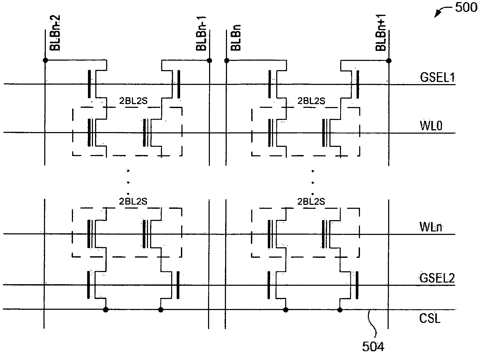
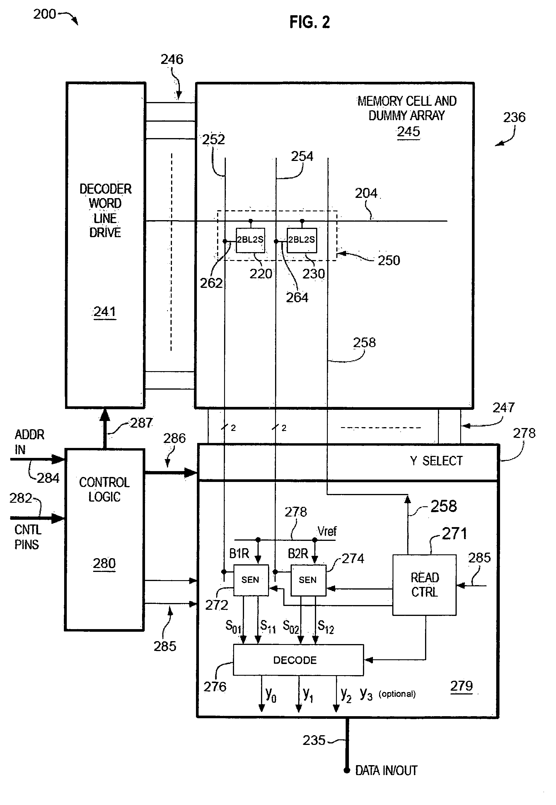
[0026]The invention relates to electronic memories. These memories include memory arrays comprising rows and columns of memory cells electrically connected with signal lines, such as word lines and bit lines, plus associated circuitry for writing and reading to the memory.

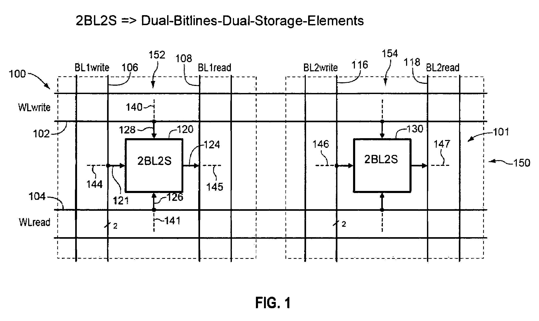
[0027]FIG. 1 shows a generalized circuit diagram illustrating the paired dual bit lines dual storage elements architecture according to the invention. Memory array portion 100 includes a cell pair 101 comprising a first dual bit lines dual storage elements cell 120 and a second dual bit lines dual storage elements cell 130. The cell has two storage elements, and the dual bit lines, e.g. 106, represent two bit lines which are normally used as true and complementary data. Each of the dual bit lines dual storage elements cell can have four logic states, “00”, “01”, “10”, and “11”. The state refers to the charge and resistance states as in each of the capacitive or resistive storage element. There are sixteen different...


PUM


Abstract

An electronic memory using true and complementary dual bit lines and dual binary storage elements cell architecture comprising a memory cell pair with four binary storage elements with each memory cell pair capable of existing in up to sixteen electronic memory states. The four binary storage elements together, normally used to store two true and complementary data bits, are used to store two, three, or four data bits depending on the noise margin allowed and bit width selection. The memory can be ferroelectric memory FeRAM, a flash memory, a ROM, a dynamic memory DRAM, an OUM, a MRAM, a NAND memory, or a NOR memory.

Description

CROSS-REFERENCE TO RELATED APPLICATIONS[0001]This patent application is a continuation-in-part under 37 CFR 1.53(b) of U.S. patent application Ser. No. 11 / 049,236 filed Feb. 2, 2005, now abandoned, which application claims the benefit of U.S. Provisional Application No. 60 / 542,094 filed Feb. 5, 2004. This application also claims the benefit of U.S. Provisional Application No. 60 / 673,399 filed Apr. 21, 2005. All of the above-referenced applications are incorporated by reference to the same extent as though fully disclosed herein.FIELD OF THE INVENTION[0002]The invention in general relates to electronic memories, and in particular, such memories capable of storing data in a plurality of binary storage elements.BACKGROUND OF THE INVENTION[0003]Electronic memories comprising arrays of memory cells arranged in rows and columns are well known. Most such memories are capable of storing a single bit of data in each memory cell. For speed, reliability, and robustness in a noisy and un-predic...

Claims


Application Information

Patent Timeline
Patent Type & Authority Patents(United States)
IPC IPC(8): G11C16/04
CPCG11C7/1006G11C7/1096G11C7/12G11C7/18G11C11/16G11C11/22G11C11/4094G11C11/4097G11C11/56G11C11/5607G11C11/5621G11C11/565G11C11/5657G11C11/5678G11C7/1078G11C2211/4013G11C13/0004G11C16/0408G11C16/0416G11C16/0441G11C16/0491G11C2211/5641H01L29/785
Inventor HO, IU-MENG TOM
Owner IOTA TECH
Features
  • R&D
  • Intellectual Property
  • Life Sciences
  • Materials
  • Tech Scout
  • Unparalleled Data Quality
  • Higher Quality Content
  • 60% Fewer Hallucinations
Learn More