Non-volatile memory device having improved program speed and associated programming method

a non-volatile memory and programming method technology, applied in static storage, digital storage, instruments, etc., can solve the problems of wasteful classification of a whole block as a bad block based on a single failed bit, and the block containing the bit is considered a bad block, so as to improve the program speed

Active Publication Date: 2008-04-01
SAMSUNG ELECTRONICS CO LTD
View PDF14 Cites 37 Cited by
  • Summary
  • Abstract
  • Description
  • Claims
  • Application Information

AI Technical Summary

Benefits of technology

[0014]Selected embodiments of the invention address the above problems by providing non-volatile memory devices wherein a memory block can be classified as a “good block” as long as a number of failed bits in the block is less than a number of bits that can be corrected by an error correction circuit. In addition, selected embodiments of the invention allow programming speed to be improved by relaxing the requirement that all cells in each memory block must be entirely programmed.

Problems solved by technology

In other words, if a bit fails to be adequately programmed after the maximum number of program loops, the block containing the bit is considered a bad block.
However, classifying a whole block as a bad block based on a single failed bit can be wasteful because often the presence of a small number of failed bits can be remedied by including an error correction circuit in the memory device.

Method used


Image

  • Non-volatile memory device having improved program speed and associated programming method
  • Non-volatile memory device having improved program speed and associated programming method
  • Non-volatile memory device having improved program speed and associated programming method

Examples


Embodiment Construction

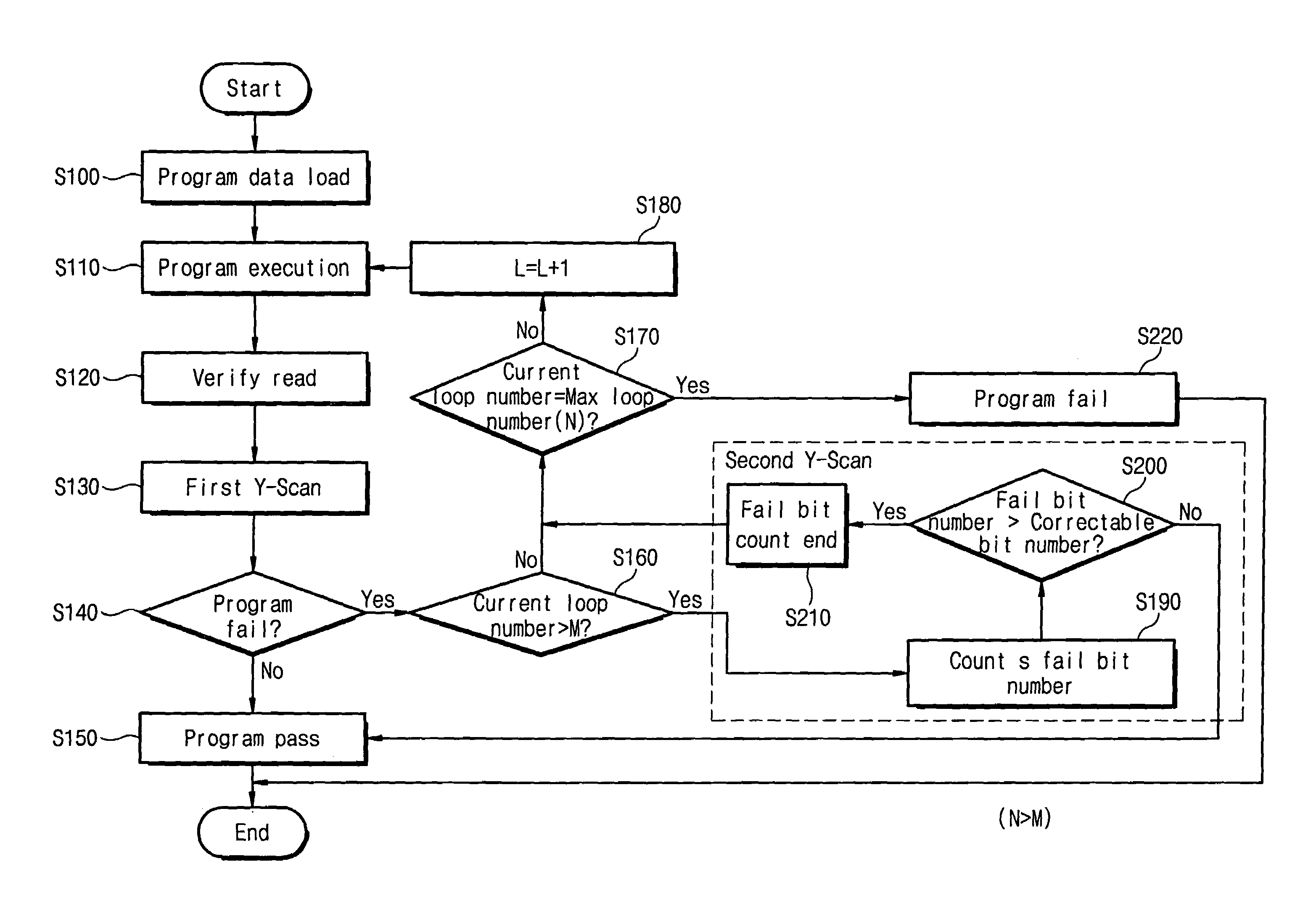
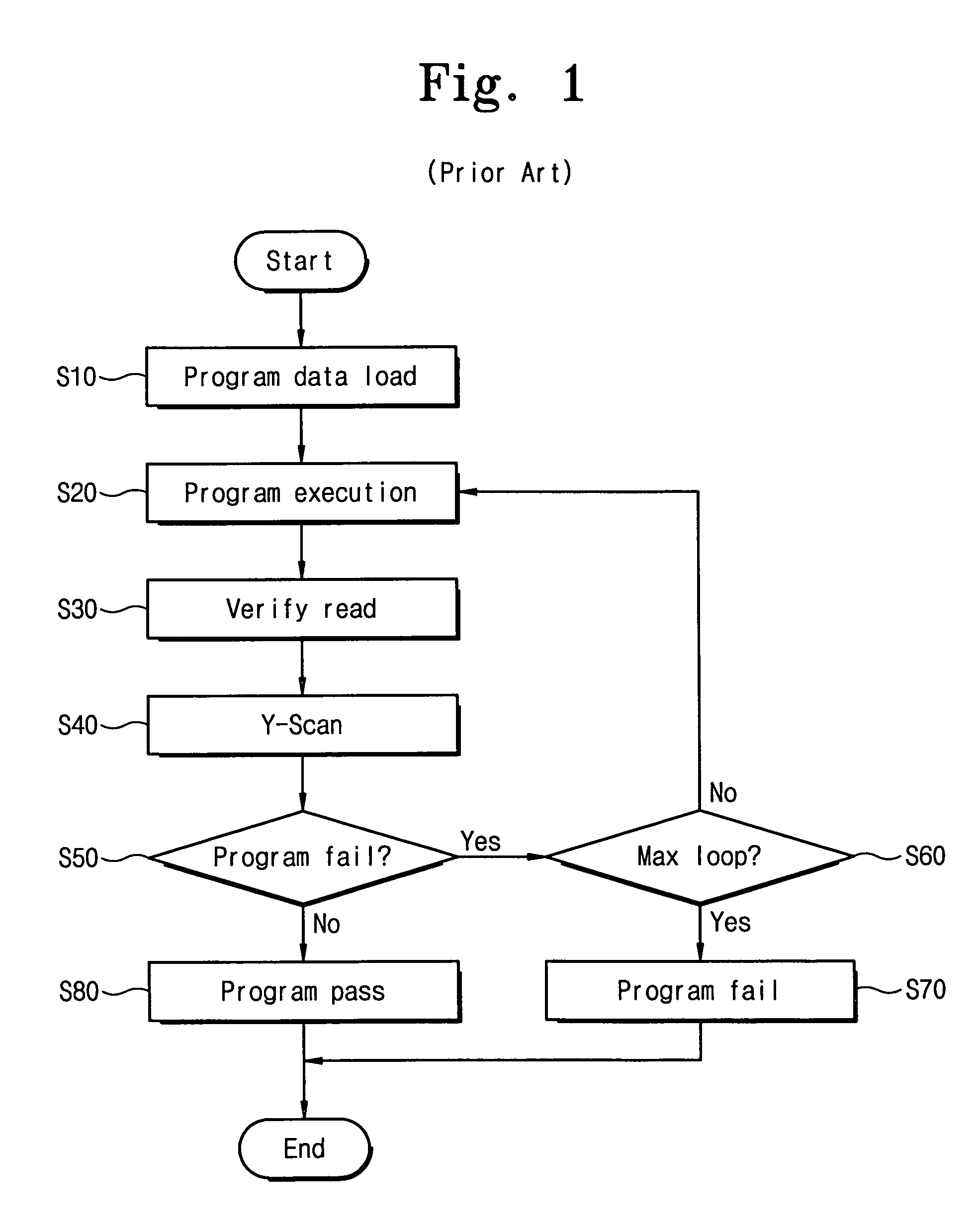
[0024]Exemplary embodiments of the invention are described below with reference to the corresponding drawings. These embodiments are presented as teaching examples. The actual scope of the invention is defined by the claims that follow.

[0025]In the description that follows, a NAND flash memory is used as an example of a non-volatile memory device to illustrate various characteristics and functions provided by certain aspects of the invention. However, those skilled in the art will understand that other types of non-volatile memories can be used without departing from the scope of the invention.

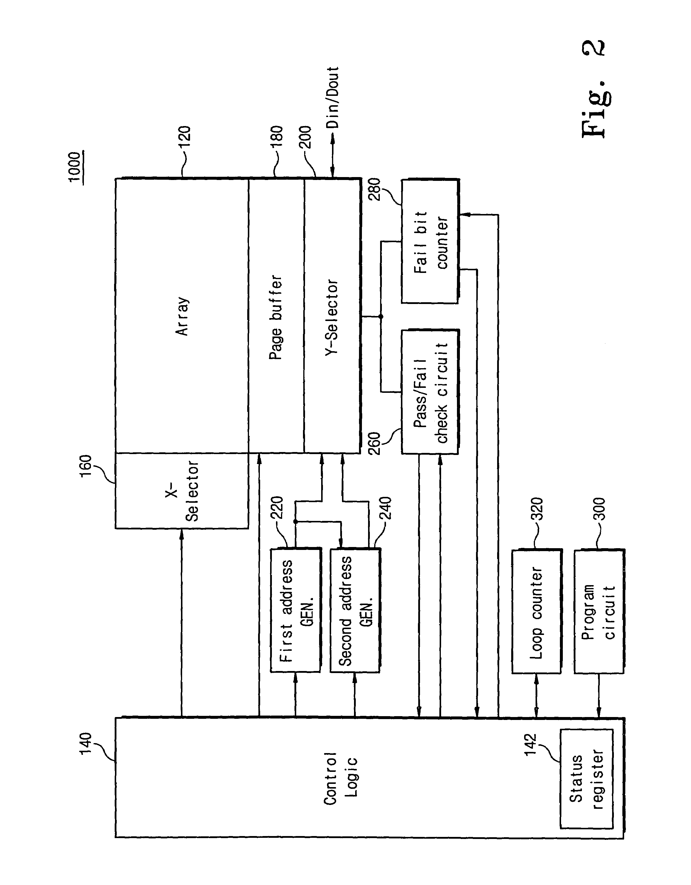
[0026]FIG. 2 is a block diagram of a non-volatile memory device 1000 according to an embodiment of the present invention. Referring to FIG. 2, non-volatile memory device 1000 comprises a memory cell array 120 comprising a plurality of non-volatile memory cells arranged in a matrix and connected to corresponding wordlines and bitlines arranged in rows and columns, respectively. The memory cells...


PUM


Abstract

A non-volatile memory device comprises a memory cell array having a plurality of non-volatile memory cells arranged in rows and columns. Selected memory cells are programmed by applying program voltages thereto. Next, data bits stored in the selected cells are read. Then, a first column scan operation is performed to determine whether any of the selected memory cells is inadequately programmed. Upon determining that at least one of the selected memory cells is inadequately programmed, a second column scan operation is performed to detect a total number of the selected memory cells that are inadequately programmed. Upon determining that the total number of the selected memory cells that are inadequately programmed is less than a number that can be corrected by an error correcting circuit, the program operation terminates with a program pass status.

Description

BACKGROUND OF THE INVENTION[0001]1. Field of the Invention[0002]Embodiments of the present invention relate generally to semiconductor memory devices. More particularly, embodiments of the invention relate to non-volatile memory devices and associated programming methods.[0003]A claim of priority is made to Korean Patent Application No. 2005-68039 filed on Jul. 26, 2005, the disclosure of which is hereby incorporated by reference in its entirety.[0004]2. Description of Related Art[0005]The demand for high performance non-volatile memory devices has increased dramatically in recent years. This increased demand is due at least in part to the proliferation of increasingly sophisticated portable electronic devices requiring high capacity, high speed memories capable of storing data even when power is cut off from the devices.[0006]Flash memory is one of the most popular forms of non-volatile memory in use today. Flash memory is a popular choice for portable electronic devices for many r...

Claims


Application Information

Patent Timeline
Patent Type & Authority Patents(United States)
IPC IPC(8): G11C11/34
CPCG11C16/3454G11C16/10
Inventor LEE, CHUL-HOLEE, JIN-YUB
Owner SAMSUNG ELECTRONICS CO LTD
Why Eureka
Try Eureka