Solid-state imaging device and camera

a solid-state imaging and camera technology, applied in the field of solid-state imaging devices, can solve the problems of deteriorating image sensitivity, aberration, color shading, sensitivity shading, etc., and achieves the effects of high light condensation rate, excellent image quality, and high image sensitivity

Inactive Publication Date: 2008-04-15
COLLABO INNOVATIONS INC
View PDF19 Cites 10 Cited by
  • Summary
  • Abstract
  • Description
  • Claims
  • Application Information

AI Technical Summary

Benefits of technology

[0016]Therefore, an object of the present invention is to provide a solid-state imaging device in which not only miniaturization of pixels but also a high light-condensing rate, a high image sensitivity, and an excellent image quality are achieved, while reducing color shading and sensitivity shading.
[0024]A solid-state imaging device according to the present invention is, more specifically, a solid-state imaging device in which incident light is received in a light-sensitive area formed in each of a plurality of pixels arranged in a matrix on a semiconductor substrate, and an electrical signal of intensity according to intensity of the incident light is outputted, the solid-state imaging device comprising: a plurality of converging lenses for deflecting the incident light in such a manner that the incident light is converged on a center of each pixel, and a plurality of light-path change portions that are each provided corresponding to one pixel and which are each used for deflecting the incident light traveling toward a center of a corresponding pixel in such a manner that the incident light is directed toward a center of a corresponding light-sensitive area, wherein, the plurality of pixels each satisfy one of a predetermined number of positional relationships between the center of the pixel and the center of the light-sensitive area when seen from directly above a principal surface of the semiconductor substrate, such that the predetermined number of neighboring pixels satisfying all of the predetermined number of positional relationships constitute one unit of pixels; each unit of pixels thus has an identical structure containing the predetermined number of neighboring pixels; and one or more light-path change portions defining one unit are formed so as to correspond to one unit of pixels. In accordance with the above structure, the light-condensing rate can be further improved. The one or more light-path change portions defining one unit may be formed astride a plurality of neighboring units of pixels.
[0027]A solid-state imaging device according to the present invention has, in at least some of the pixels, light-path change portions for deflecting incident light that travels toward the centers of their corresponding pixels in such a manner that the incident light is directed toward the centers of the light-sensitive areas. Therefore, even if a solid-state imaging device is structured such that the centers of light-sensitive areas are offset from the centers of their corresponding pixels when seen from directly above a principal surface of the semiconductor substrate in order to achieve the miniaturization of pixels, a high light-condensing rate can be achieved. As a result, a solid-state imaging device in which miniaturization of pixels and a high image quality are achieved at the same time is provided.

Problems solved by technology

However, although miniaturization of pixels 2 is realized, the solid-state imaging device shown in FIG. 12 has a problem in that the light-condensing rate with respect to the entire solid-state imaging device becomes lower.
As a result, aberration, color shading, sensitivity shading, the deterioration of image sensitivity, and the like occur.
In this case, however, because as described above the centers p of the light-sensitive areas 3 on the substrate are not arranged at regular intervals, the configuration of converging lenses 10 would inevitably become complicated.
Therefore, the entire area of the pixel 2 could not be utilized efficiently.

Method used


Image

  • Solid-state imaging device and camera
  • Solid-state imaging device and camera
  • Solid-state imaging device and camera

Examples


Embodiment Construction

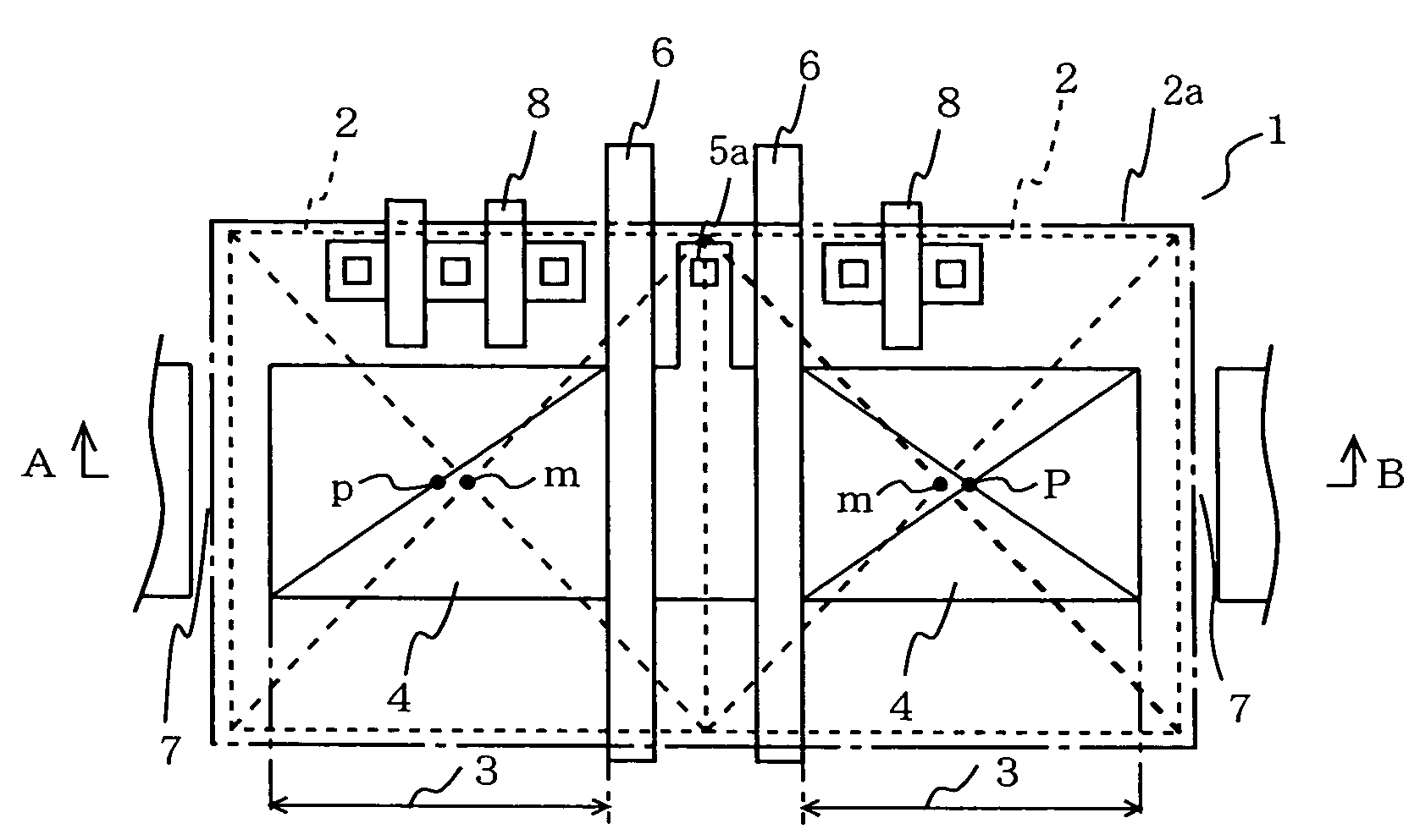
[0049]A solid-state imaging device according to an embodiment of the present invention is described below with reference to the accompanying figures, illustrating an exemplary solid-state imaging device in which every two pixels define one cell.

[0050]FIG. 1 is a schematic top plan view for illustrating positional relationships between pixels and light-sensitive areas of a solid-state imaging device in which a plurality of pixels are arranged in a two-dimensional arrangement, e.g., a matrix.

[0051]The solid-state imaging device shown in FIG. 1 includes a semiconductor substrate 1, pixels 2, and light-sensitive areas 3. As the semiconductor substrate 1, a p-type silicon substrate is generally used. On the semiconductor substrate 1, a plurality of pixels 2 are arranged in a matrix and, in addition, units 2a of pixels, each unit 2a of pixels being constituted by two pixels defining one cell (unit), are constructed. Herein, the pixels 2 and the units 2a of pixels are shown as projections ...


PUM


Abstract

A solid-state imaging device includes pixels 2 arranged two-dimensionally on a semiconductor substrate 1. In a predetermined area in each pixel is formed a light-sensitive area 3 for receiving incident light 11, and each pixel includes a photoelectric conversion portion 4 for converting the incident light into a signal charge. In at least some of the pixels, the center of the light-sensitive area is offset from the center of the pixel when seen from directly above a principal surface of the semiconductor substrate. Each pixel further includes a light-path change member 12a and 12b for deflecting incident light traveling toward the center of the pixel so as to be directed toward the center of the light-sensitive area. Thus, a solid-state imaging device simultaneously realizing the miniaturization of pixels and a high image quality is provided.

Description

BACKGROUND OF THE INVENTION[0001]1. Field of the Invention[0002]The present invention relates to a solid-state imaging device. More particularly, the present invention relates to a solid-state imaging device in which a plurality of pixels are arranged in a matrix and to a camera utilizing the same.[0003]2. Description of the Background Art[0004]In a solid-state imaging device such as CCD and MOS image sensors, it is required to increase the light-condensing rate in order to improve image quality. To increase the light-condensing rate, a converging lens is used in general. With reference to the accompanying figures, a common structure of a solid-state imaging device will be described below.[0005]FIG. 9 is a schematic top plan view for illustrating the positional relationship between pixels and light-sensitive areas in a solid-state imaging device in which a plurality of pixels are arranged in a matrix.[0006]The solid-state imaging device illustrated in FIG. 9 includes a semiconductor...

Claims


Application Information

Patent Timeline
Patent Type & Authority Patents(United States)
IPC IPC(8): H01L27/00H04N5/225H01L27/14G02B3/00H01L27/146H01L31/0232H01L31/10H04N5/335H04N5/361H04N5/369H04N5/372H04N5/374
CPCH01L27/14601H01L27/14685H01L27/14627H01L27/14625H01L27/14603H01L27/14605H01L27/14H01L31/10H01L27/146
Inventor TANAKA, SYOUJIMIYAGAWA, RYOHEIFUJII, TOSHIYATANAKA, YASUHIROYAMAGATA, MICHIHIROOKAYAMA, HIROAKI
Owner COLLABO INNOVATIONS INC
Why Eureka
Try Eureka