Display device

a display device and display technology, applied in the field of display devices, can solve the problems of degrading light utilization efficiency, high cost, difficult manufacturing and high cost, etc., and achieve the effects of high resolution, high resolution, and strong light absorption property

Inactive Publication Date: 2008-04-29
FUJIFILM CORP +1
View PDF9 Cites 2 Cited by
  • Summary
  • Abstract
  • Description
  • Claims
  • Application Information

AI Technical Summary

Benefits of technology

[0028]In such structure, the light transmitted through the first reflector and entered into the translucent porous body repeats reflections between the first and second reflectors, causing multipath refection to occur effectively. This causes multipath reflection interference to be developed effectively, and the light absorption property for absorbing light having a particular wavelength is produced. The input light is modulated by the light absorption effect and the modulated light is outputted from the first reflector and / or the second reflector.
[0030]The display device of the present invention has a strong light absorption property for a particular wavelength due to multipath interference. This allows high resolution optical modulation to be performed with respect to each display dot. Further, the device has a structure which is substantially smaller than the wavelength of the input light as the smallest optical modulation unit, and a single display dot may be constituted by a single or a plurality of pores having a diameter which is substantially smaller than the wavelength of the input light. Thus, according to the present invention, a display device with high resolution and high display quality may be provided.
[0031]The display device of the present invention structurally has a wavelength selection capability, so that it may perform image display without using any polarizer, and provide full color display without using any color filter. That is, the display device has higher light utilization efficiency than the conventional liquid crystal device.

Problems solved by technology

The conventional interference filters require a high degree of smoothness and accuracy for the thickness of the film, making them difficult to manufacture and requiring high costs, in particular, those with large display area.
Thus, different interference filters are required for different wavelengths to be absorbed (transmitted), which has been an obstacle for flexibly responding to design changes in optical systems.
Each of the optical modulation devices described in the aforementioned patent publications may alter the optical modulation property by changing the fluid filled therein, but it is difficult for them to achieve fine and high resolution optical modulation.
Thus, a certain amount of light is absorbed by the polarized, and the light utilization efficiency is degraded by that much.
Further, in order to provide full color display using the liquid crystal device, a color filter is required which absorbs a certain amount of light and the light utilization efficiency is degraded by that much.

Method used


Image

  • Display device
  • Display device
  • Display device

Examples


first embodiment

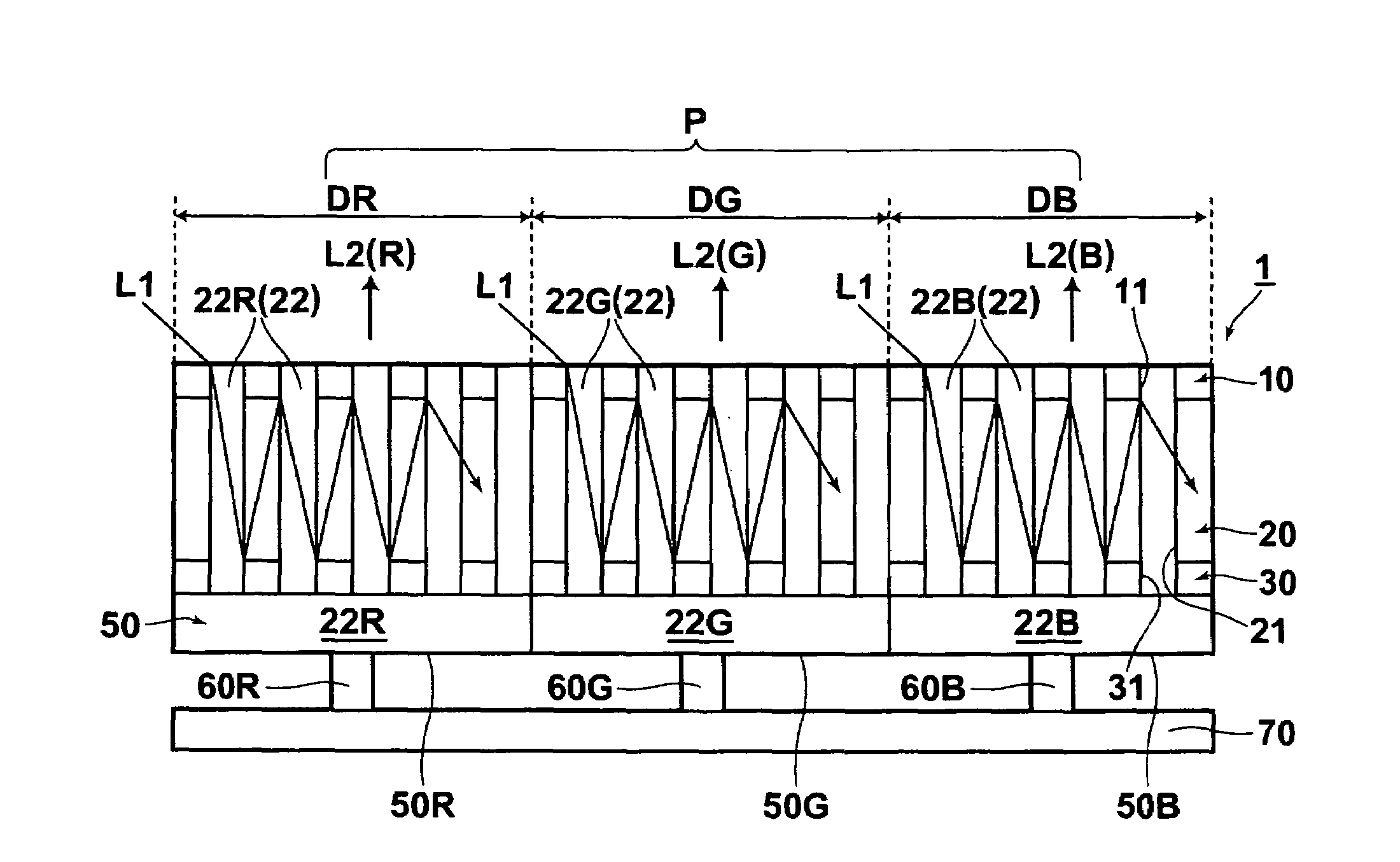
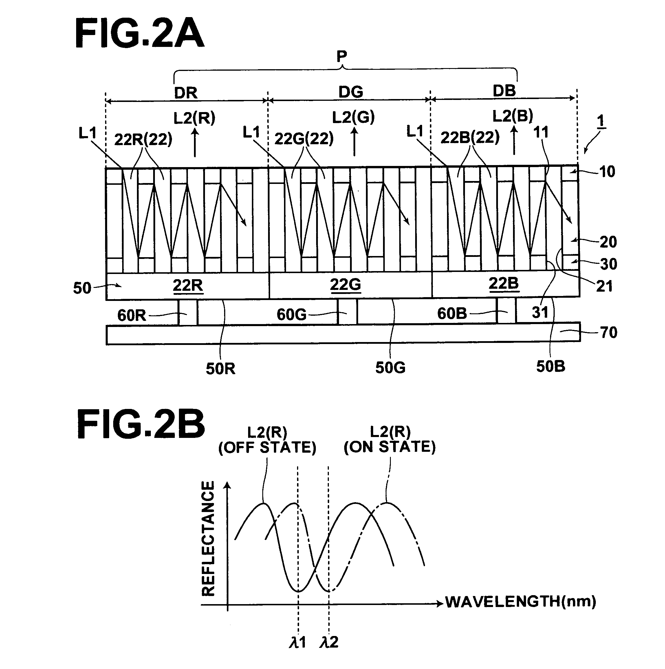
[0042]Hereinafter, the structure of the display device according to a first embodiment of the present invention will be described with reference to FIGS. 1 to 3. FIG. 1 is a plan view illustrating the pixel pattern of the present display device 1. FIG. 2A is a thickness cross-sectional view of a single pixel of the display device 1 according to the present embodiment (hatching is omitted). FIG. 2B shows example spectra of the modulated light. FIGS. 3A to 3C are drawings (perspective views) illustrating the manufacturing process of the display device 1 according to the present embodiment.

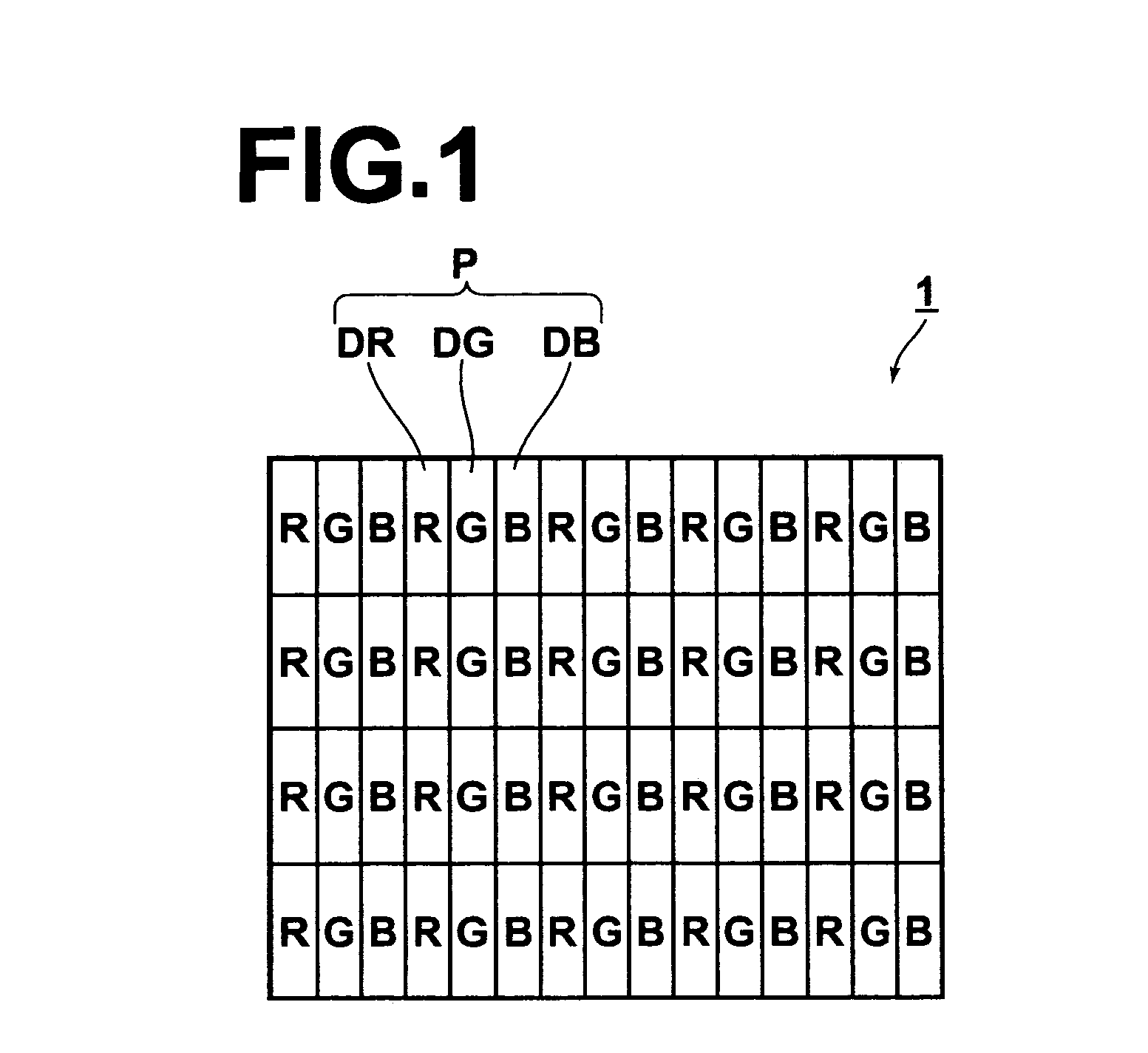
[0043]As shown in FIG. 1, the display device 1 according to the present embodiment is a full color device with multitudes of pixels disposed in a matrix. Each of the pixels includes a display dot DR for outputting red light (within a wavelength range from 625 to 740 nm), a display dot DG for outputting green light (within a wavelength range from 500 to 565 nm), and a display dot GB for outputting blu...

second embodiment

[0094]Hereinafter, the structure of the display device according to a second embodiment of the present invention will be described with reference to FIGS. 4A to 4C. The basic structure of the present embodiment is identical to that of the first embodiment. Therefore, identical components are given the same reference symbols and will not be elaborated upon further here. FIG. 4A is a cross-sectional view of the present embodiment corresponding to FIG. 2A in the first embodiment. FIG. 4B shows example spectra of the modulated light (before bandpass filter), and FIG. 4C is an example spectrum illustrating the transmission characteristics of a bandpass filter. In the present embodiment, a reflective type device will be described as an example.

[0095]As shown in FIG. 4A, the display device 2 according to the present embodiment includes a bandpass filter (BPF) 80 provided on the light output side (on the side of the first reflector 10) of the display device 1 according to the first embodime...

third embodiment

[0100]Hereinafter, the structure of the display device according to a third embodiment of the present invention will be described with reference to FIGS. 5A and 5B. The basic structure of the present embodiment is identical to that of the first embodiment. Therefore, identical components are given the same reference symbols and will not be elaborated upon further here. FIG. 5A is a cross-sectional view of the present embodiment corresponding to FIG. 2A in the first embodiment, and FIG. 5B is a top view (viewed from the side of the first reflector 10) of the display device shown in FIG. 5A, illustrating the device when displaying an image.

[0101]The display device 3 according to the present embodiment has a device structure that includes the following arranged from the light input side (upper side in FIG. 5A) in the order listed below: the first reflector 10; translucent porous body 20; and second reflector 30 as in the first embodiment. In the display device 3, however, the pores 21 ...


PUM

PropertyMeasurementUnit
diameteraaaaaaaaaa
wavelength rangeaaaaaaaaaa

Abstract

A display device comprising the following arranged from light input side in the order listed below: a first reflector having a semi-transmissive and semi-reflective property; a translucent porous body having a plurality of pores in which a translucent material is filled, each of the pores having a substantially smaller diameter than the wavelength of input light; and a second reflector having a perfect reflection property, or a semi-transmissive and semi-reflective property. The average complex refractive index of the translucent porous body is changeable with respect to each display dot, and the wavelength of light absorbed by the translucent porous body is changeable with respect to each display dot according to the average complex refractive index. In this way, the input light is modulatable, and the modulated light is outputted from the first reflector and / or the second reflector to perform image display.

Description

BACKGROUND OF THE INVENTION[0001]1. Field of the Invention[0002]The present invention relates to a display device that performs image display by modulating input light with respect to each display dot and outputting the modulated light.[0003]2. Description of the Related Art[0004]As one of the optical modulation devices that modulate light by absorbing light having a particular wavelength, interference filters, such as etalon filter and the like, are put into practical use. The conventional interference filters require a high degree of smoothness and accuracy for the thickness of the film, making them difficult to manufacture and requiring high costs, in particular, those with large display area. In addition, the optical modulation property is fixed due to the rigid structure. Thus, different interference filters are required for different wavelengths to be absorbed (transmitted), which has been an obstacle for flexibly responding to design changes in optical systems.[0005]Under the...

Claims


Application Information

Patent Timeline
Patent Type & Authority Patents(United States)
IPC IPC(8): G02F1/03G02F1/29G09F19/00G09F19/14G09G3/34
CPCG02B26/001G02F1/133553G02F1/133509G02F1/21G02F2202/32
Inventor TOMARU, YUICHI
Owner FUJIFILM CORP
Why Eureka
Try Eureka