
Optical fiber component package for high power dissipation

a technology of optical fiber and component package, applied in the field of optical fiber component package, can solve the problems of inability to solve component related power handling problems, inability to use optical fiber based loss extraction, and limited power levels for most applications, so as to maximize thermal conductivity, minimize reflection, and maximize the effect of effective dissipation

Active Publication Date: 2008-05-13
ITF TECH
View PDF4 Cites 49 Cited by
  • Summary
  • Abstract
  • Description
  • Claims
  • Application Information

AI Technical Summary

Benefits of technology

[0007]A further object of the present invention is to provide an optical fiber component package that will avoid damage to the optical fiber device due to mechanical stresses.
[0015]The same concerns apply to the signal-carrying fiber, especially in the case of large mode area fibers, where low numerical apertures and large V numbers make splicing an important source of modal degradation. Increased LP01 loss not only generates heat loads, but also can result in a non-thermally driven failure mode. As more interfering modes are excited, gain instabilities can lead to the generation of intense pulses that will exceed the material breakdown threshold of glass, resulting in destruction of the core, typically in the regions of smallest mode diameter. It is not the purpose of a packaging solution to solve this issue, however, the coupler package should preserve modal quality during assembly and subsequently in all conditions of use, including laser power cycling and ambient temperature cycling.
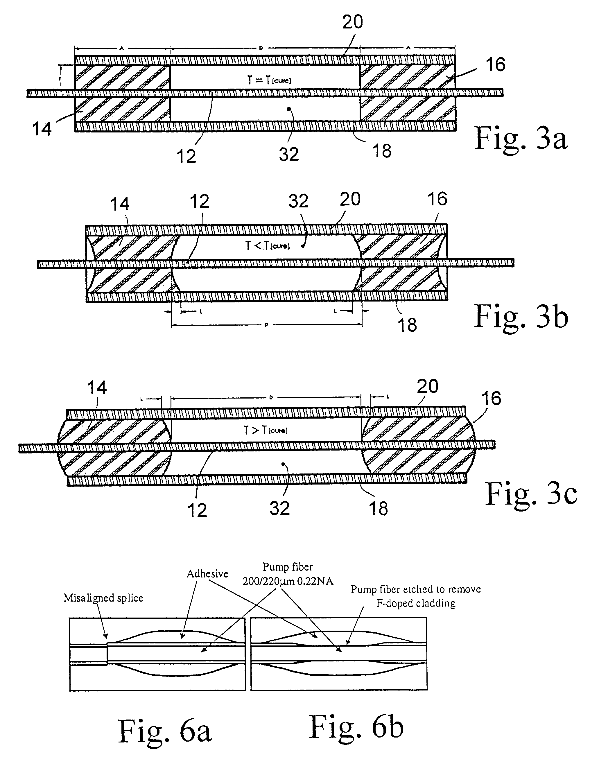
[0019]β=P0⁢αkA⁡(α2-λ2)⁢⁢and⁢⁢λ2=2⁢hkrEquation 4 predicts a longitudinal profile where a peak is present some distance away from the edges of the bondline. It is important to locate this point in order to properly establish the maximum temperature reached during operation. In order to corroborate the model, samples were instrumented to provide temperature-mapping capability inside a fully enclosed package. Capillary tubing transecting the adhesive bond in the radial and longitudinal axis were introduced to allow high reflectivity Bragg gratings to be positioned for profiling. To produce a well-controlled optical loss function, a length of pump fiber was stripped and etched in hydrofluoric acid to expose its core to mode stripping from the adhesive. A match was shown between the fitted theoretical profile and the temperature reading from the Bragg. In the radial profile, most heat is generated close to the fiber, probably because the refracted signal has a strong forward directionality. This measurement also confirms that the sidewalls of the package are indeed acting as heatsinks, the distribution matching closely the package sidewall diameter of 3 mm. This analysis indicates that the best strategy to decrease temperature elevation in the package is to control and preferably to minimize the length and diameter of the adhesive, select an adhesive with good transparency and make it contact a packaging material with good thermal conductivity. Also, the packaging material should be such as to compensate for any variation of the adhesive bond at each end of the package, due to temperature variation, so as to prevent damage to the optical device by mechanical stresses that may otherwise be produced.
[0025]The packaging substrate should preferably have a high thermal conductivity and an absorption capacity such as to absorb essentially all optical loss emanating from the optical fiber device when it is in operation. It may consist of metal or alloy (e.g. CuW or CuMo), or a metal composite (e.g. AlSi), or an advanced composite material (pyrolated graphite), or a ceramic (e.g. AlN), or it can be a combination of two materials in a bi-material arrangement (e.g. Invar or Kovar with inserts of Cu, Ag or Al), or a combination of the above with a highly conductive layer (e.g. electroplated, hot dipped, thin film or foil). Normally, the thermal conductivity should be at least 100 w / mk (watts / meter-kelvin), and preferably it should be higher than 130 w / mk. Normally, the packaging is opaque because this allows the spurious optical signal to be directly absorbed and dissipated, and thus offers an efficient heat extraction and protection against exposure to damaging optical power.
[0029]The surface of the inner walls of the packaging substrate may be treated to minimize reflections and maximize effective dissipative power of the package. This can be done by abrasion, oxidation or thin film coating or a combination thereof. The finish of the outside surfaces is preferably designed to maximize thermal conductivity. The package produced is preferably flat and rectangular to allow efficient thermal contact when mounting to a flat surface; Also, grooved channels on each side of the package wall are normally provided to allow clamping down with a variety of fasteners and a precise positioning of the component into a complete assembly, providing means to finely adjust its position with respect to other components in the assembly. This also allows CTE mismatches between package and mounting surface to be resolved through pistonning. Finally, strain relief shapes may be machined into the ends of the channels to avoid the use of more conventional elastomeric boots, which may be susceptible to degradation.

Problems solved by technology

Power levels for most applications have however been limited to the range of a few tens of Watts.
These two inventions specifically address the issue of power handling of the optical fiber and its coating, but do not provide a solution for the component related power handling issues.
In general optical loss will be spurious in nature and the corresponding optical beam characteristics will be ill-defined, which makes the use of an optical fiber based loss extraction impractical.
However, little progress has been made or improvements proposed for increasing the power handling capabilities of these components.

Method used


Image

  • Optical fiber component package for high power dissipation
  • Optical fiber component package for high power dissipation
  • Optical fiber component package for high power dissipation

Examples


Embodiment Construction

[0038]Preferred embodiments of the invention will now be described with reference to the appended drawings.

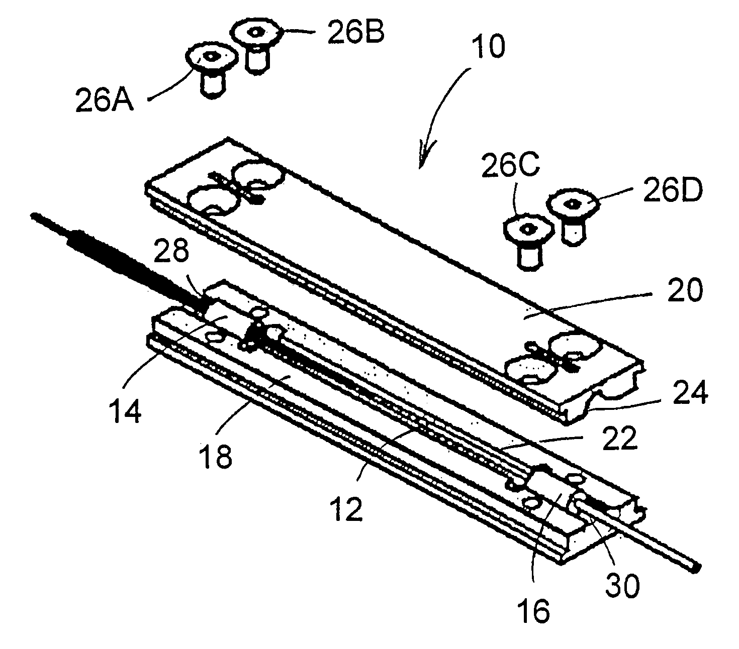
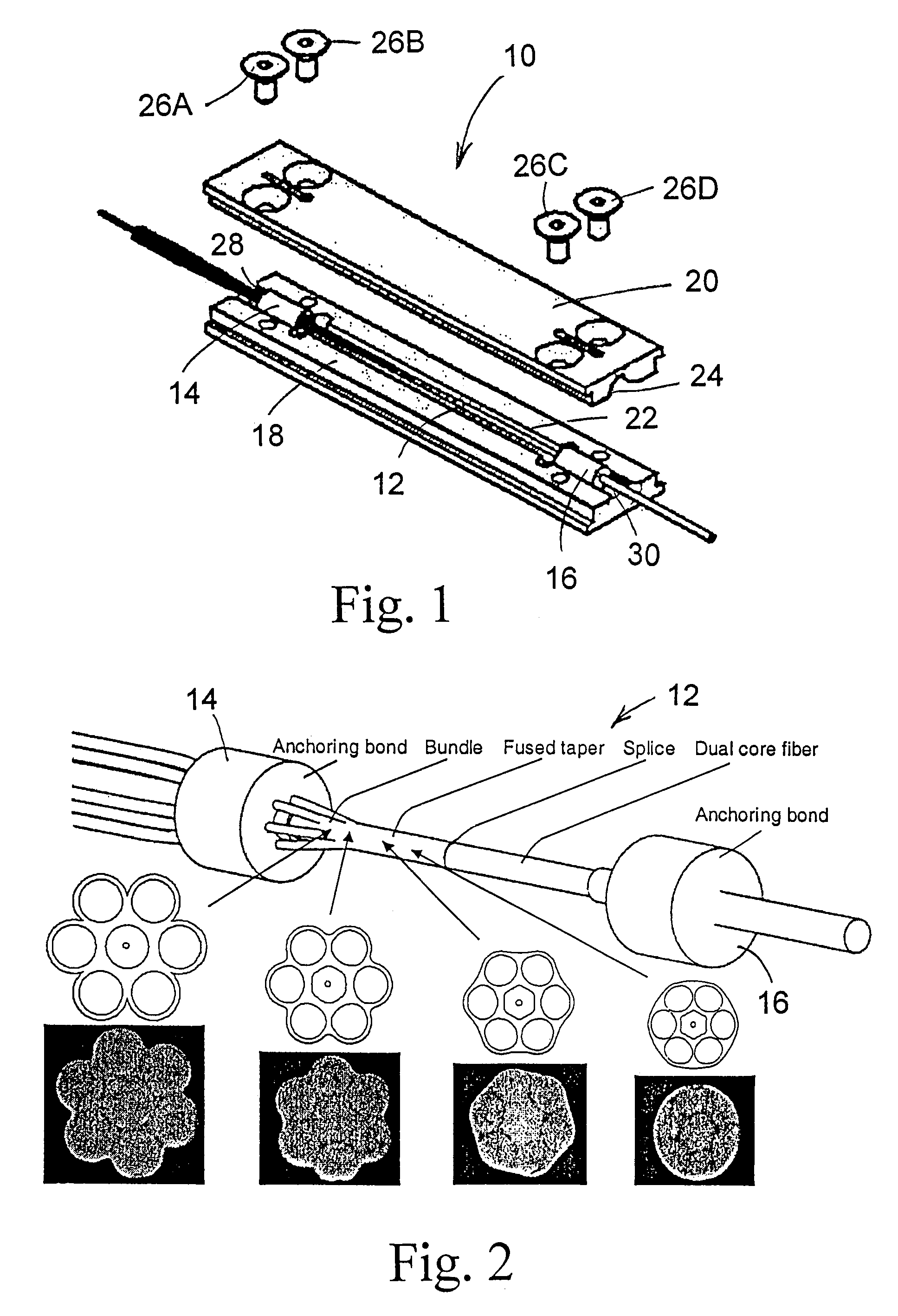
[0039]FIG. 1 illustrates a preferred design of the package 10 for an optical fiber device 12 packaged in accordance with the present invention. The optical fiber device 12 in this embodiment is a tapered fused bundle (TFB) coupler used to combine signal and pump power, which is illustrated in greater detail in FIG. 2, although it may be any device capable of carrying a high power signal. At each end, the TFB is anchored by means of an adhesive bond 14 and 16 respectively to a packaging substrate consisting of lower and upper sections 18 and 20 respectively. Each section is provided with a grooved channel 22 and 24 respectively in which the device 12 is packaged when the two sections are fastened to one another, for example by means of screws 26A, 26B, 26C and 26D. Strain relief shapes 28, 30 are provided at each end of the device 12 applied to the ends of channel 22 and similar...


PUM

PropertyMeasurementUnit
thicknessaaaaaaaaaa
transparencyaaaaaaaaaa
temperatureaaaaaaaaaa

Abstract

A package for an optical fiber device is disclosed. It has a high thermal conductivity packaging substrate surrounding the optical fiber device and has adhesive bonds at each end anchoring the optical fiber device to the substrate. The adhesive bonds are made of a material that has high transparency in damp heat as well as a high glass transition temperature and is capable of withstanding temperatures of over 100° C. The packaging substrate has a high absorption capacity and a CTE in relation to the CTE of the adhesive bond, such as to compensate for any variation in the adhesive bond due to temperature variations. This allows to limit mechanical stress in the optical fiber device within the package.

Description

FIELD OF THE INVENTION[0001]This invention relates to an optical fiber component package. More particularly, it relates to a package for optical fiber devices that are capable of operating at high power levels.BACKGROUND OF THE INVENTION[0002]Fiber lasers and amplifiers are being used in a growing number of applications. As these mature in the commercial, deployment, an intense focus is being put on their reliability and that of their components. With the current progress in this field, reliability demonstrations must be made at increasingly higher power levels. Optical fiber reliability, connector reliability and susceptibility of optical fiber coatings to optical power damage have been studied for a number of years. Power levels for most applications have however been limited to the range of a few tens of Watts.[0003]In U.S. Pat. No. 4,678,273 a high power optical fiber with improved covering is described. In U.S. Patent Application Publication No. 2004 / 0175086 a fiber with a mult...

Claims


Application Information

Patent Timeline
Patent Type & Authority Patents(United States)
IPC IPC(8): G02B6/00
CPCG02B6/0218G02B6/36G02B6/14G02B6/2835G02B6/3636
Inventor WETTER, ALEXANDRESEGUIN, FRANCOISMARTINEAU, LILIANFAUCHER, MATHIEU
Owner ITF TECH
Learn More