

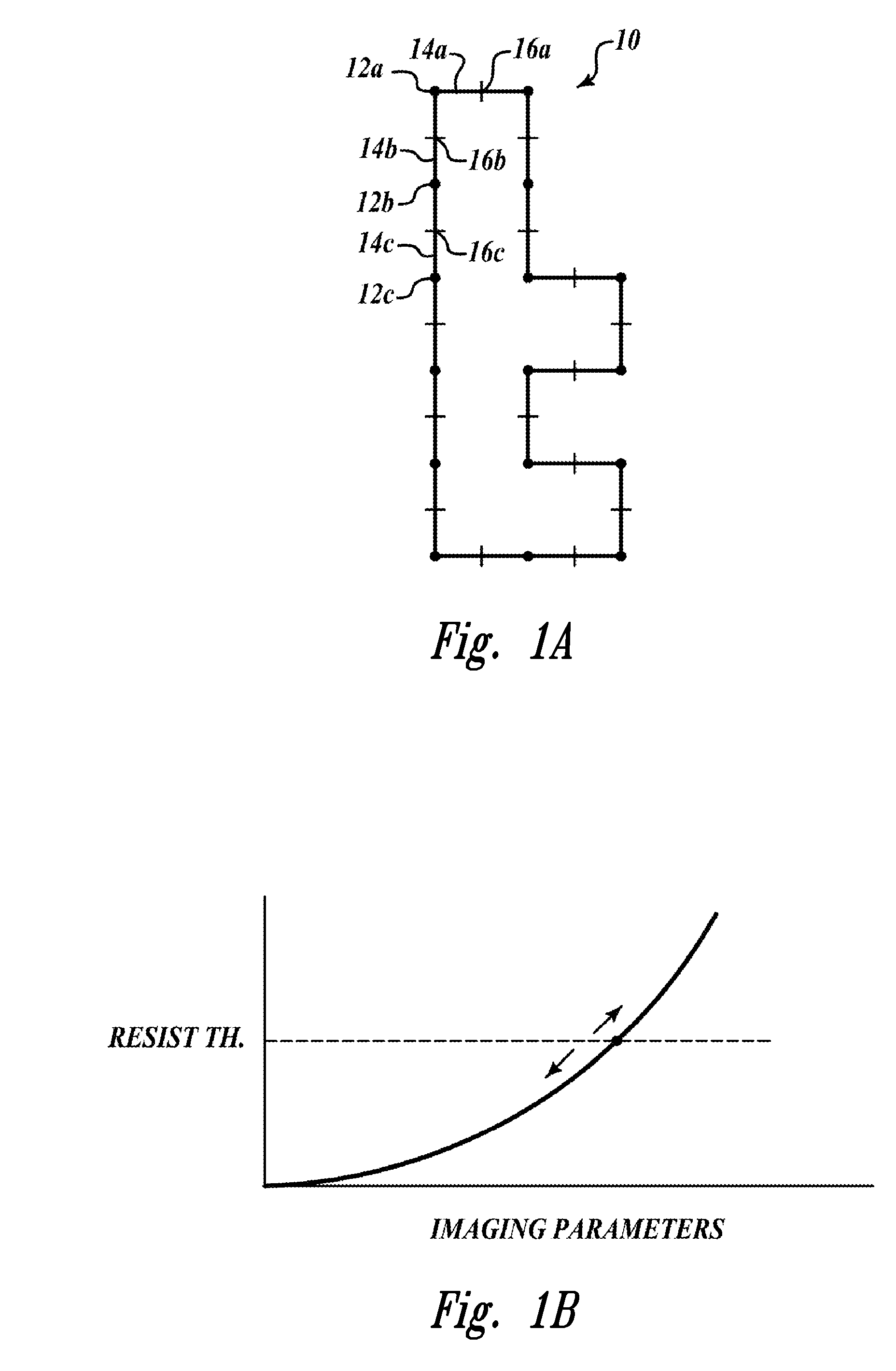
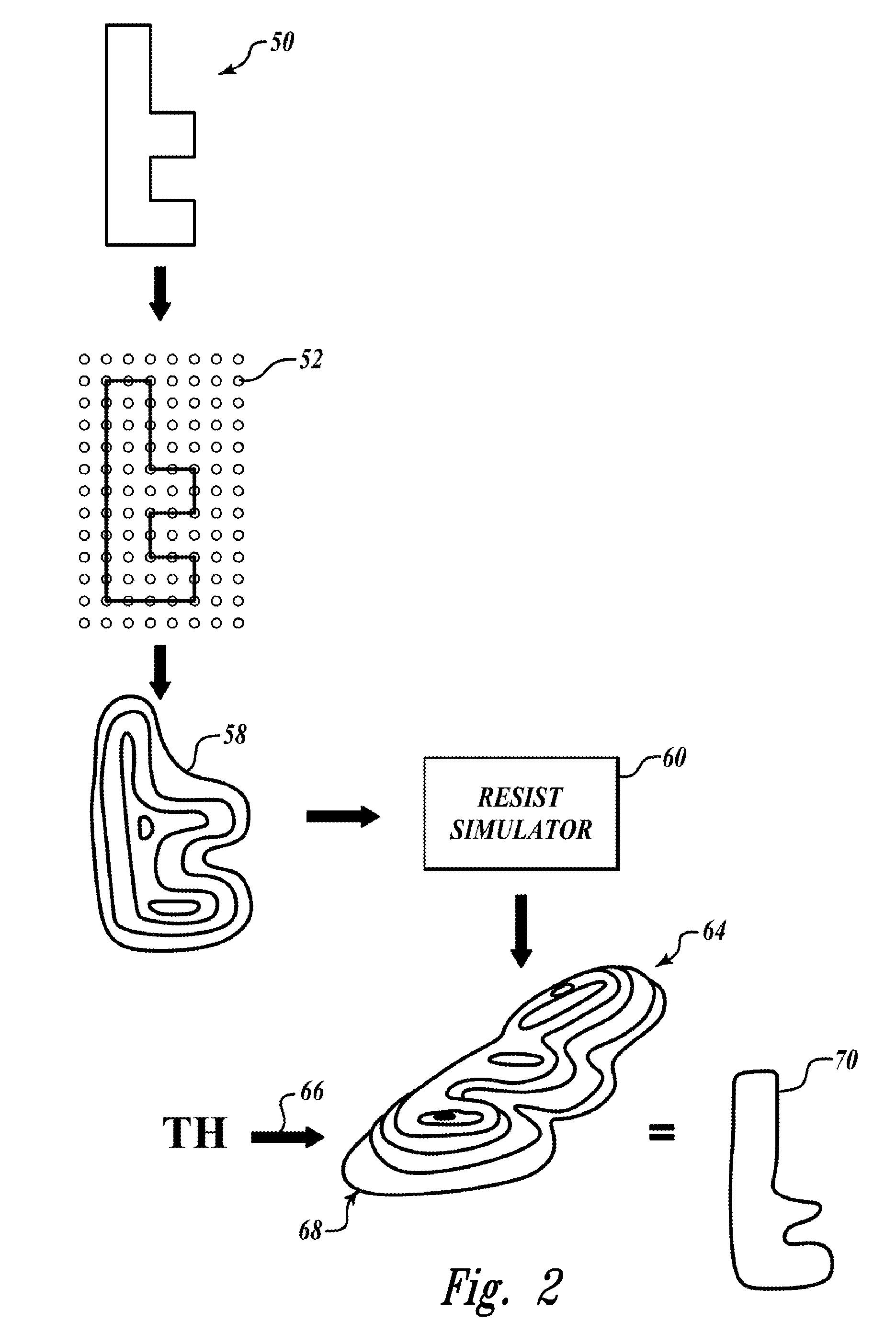
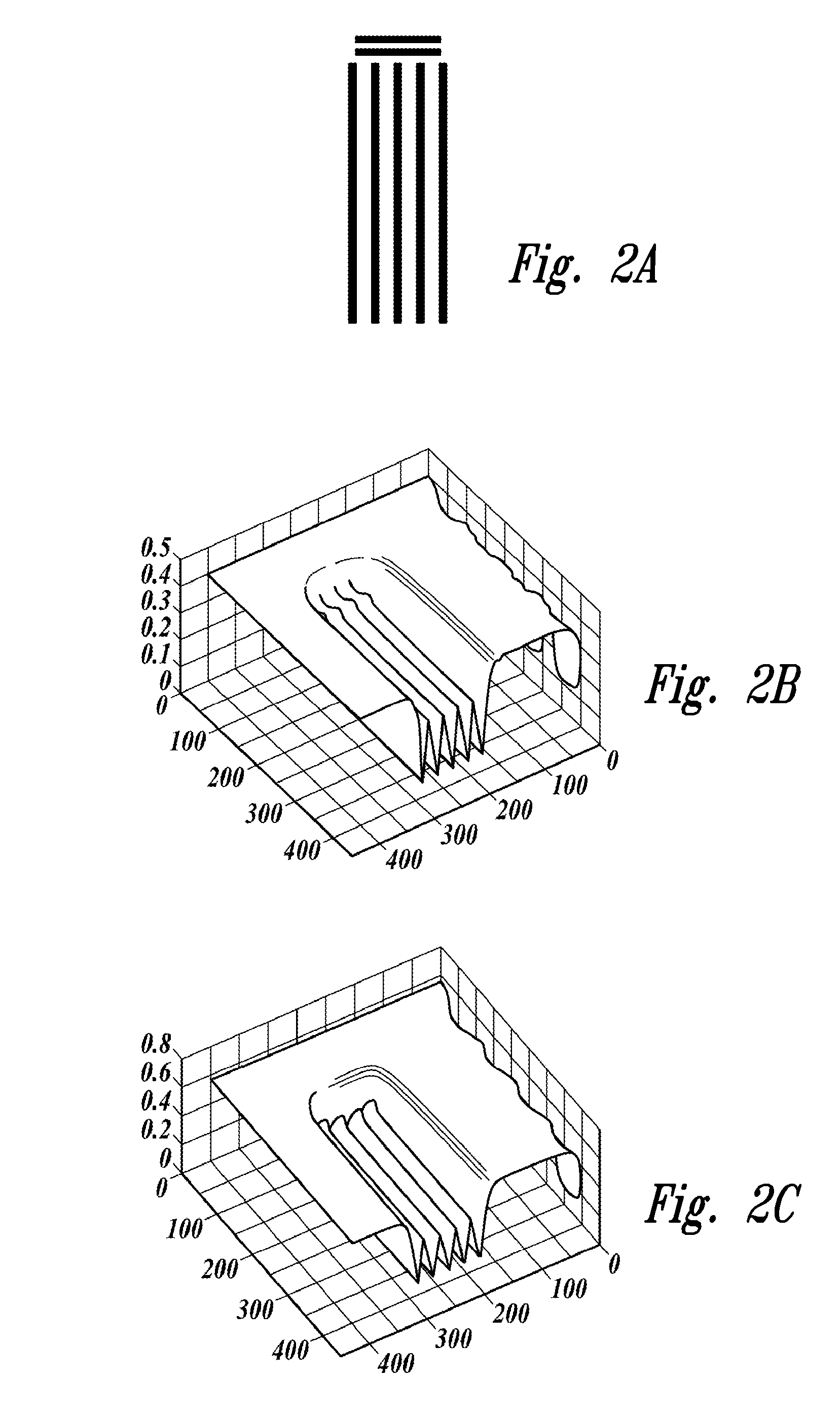
Grid-based resist simulation
a resist simulation and grid technology, applied in the field of photolithographic processing, can solve problems such as optical and other process distortions, and achieve the effect of increasing fidelity and accurate representation of expected resist behavior
- Summary
- Abstract
- Description
- Claims
- Application Information
AI Technical Summary
Benefits of technology
Problems solved by technology
Method used
Image

Examples
example
[0169]#Comments are here
[0170]version 5
[0171]modelType CM1
[0172]DEFINE M0+b=0.1 n=1 s=40 p=0
[0173]DEFINE M1−b=0.2 k=1 n=2 s=33
[0174]DEFINE M2 s=10
[0175]ANCHOR 0
[0176]COEFMAX 0.2
[0177]THRESHOLD 0.25
[0178]MCOEF 0 1
[0179]MCOEF 1 0.01
[0180]MCOEF 2−0.01
Calibration Templates
[0181]In one embodiment of the invention, the software that implements the resist simulator uses calibration templates for ease of use. The templates specify which b and s and in what range have to be calibrated. Format:
[0182]
OPTIMIZE {. . .}
[0183]The rows are numbered starting from 1.
Methodological Remarks
[0184]At the lowest level of interpretation, the resist simulator
[0185]∑iciMi(I)=T(41)
[0186]is just a mathematical calculation engine, with no or little intrinsic physical meaning. To give the model meaning as it applies to predicting the behavior of resist layers on a wafer, simulation blocks, which combine related physical parameters, are put onto the simulator. In the resist simulator according to one embodimen...
PUM
| Property | Measurement | Unit |
|---|---|---|
| size | aaaaa | aaaaa |
| size | aaaaa | aaaaa |
| width | aaaaa | aaaaa |
Abstract
Description
Claims
Application Information