Dual direction ESD clamp based on snapback NMOS cell with embedded SCR
a technology of esd clamps and snapback nmos cells, applied in semiconductor devices, semiconductor/solid-state device details, diodes, etc., can solve problems such as reverse biased current paths that cannot be provided
- Summary
- Abstract
- Description
- Claims
- Application Information
AI Technical Summary
Benefits of technology
Problems solved by technology
Method used
Image

Examples
Embodiment Construction
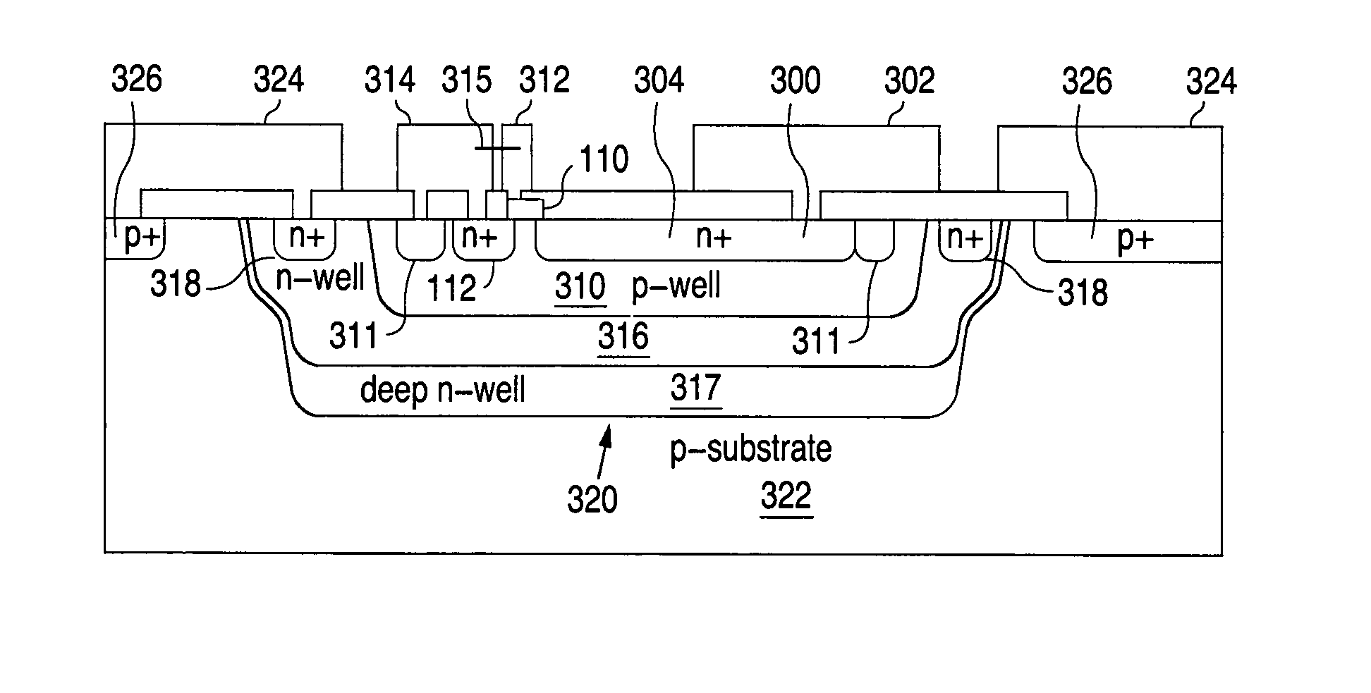
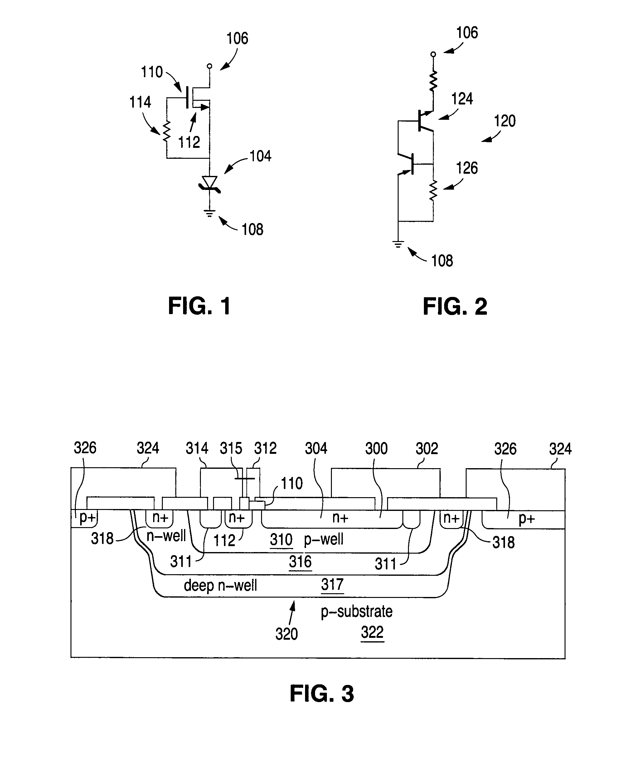
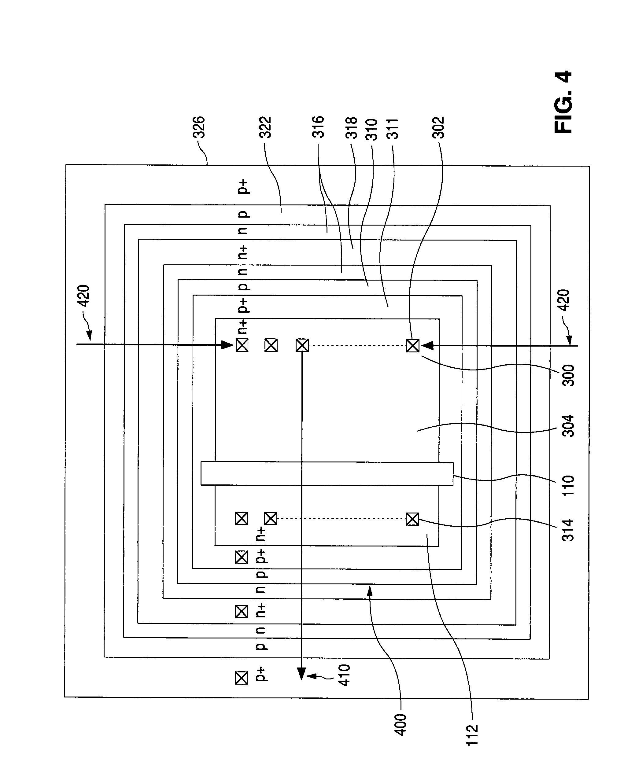
[0010]FIGS. 1 and 2 show schematic representations of the forward bias protection structure and the reverse bias protection structure, respectively of a dual direction ESD clamp of the invention.
[0011]The forward bias ESD protection structure comprises an NMOS device 102. The NMOS device 102 is shown connected in series with a diode 104, which is forward biased and thus does not interfere with the current path from the pad 106 to ground 108. (The purpose of the diode 104 will become clearer from the discussion below of the structure of the full dual direction ESD clamp.) As shown in FIG. 1, the drain of the NMOS device 102 is connected to the pad 106 and the source 112 is connected to ground via the diode 104. The gate 110 of the NMOS is connected to the source 112 through a resistor 114 so as to provide dynamic coupling between the gate and the source. The source 112 is also connected to the substrate of the device to define a high voltage tolerant NMOS structure. The substrate of ...
PUM
 Abstract
Description
Claims
Application Information
 - R&D
- Intellectual Property
- Life Sciences
- Materials
- Tech Scout
- Unparalleled Data Quality
- Higher Quality Content
- 60% Fewer Hallucinations
Browse by: Latest US Patents, China's latest patents, Technical Efficacy Thesaurus, Application Domain, Technology Topic, Popular Technical Reports.
© 2025 PatSnap. All rights reserved.Legal|Privacy policy|Modern Slavery Act Transparency Statement|Sitemap|About US| Contact US: help@patsnap.com