Structure for and method of using a four terminal hybrid silicon/organic field effect sensor device

a sensor device and hybrid technology, applied in the field of hybrid composite silicon/organic field effect sensors, can solve the problems of low sensitivity of the device, reliability problems, and difficulty in “resetting” the devi

Inactive Publication Date: 2008-07-08
BOARD OF RGT THE UNIV OF TEXAS SYST
View PDF14 Cites 29 Cited by
  • Summary
  • Abstract
  • Description
  • Claims
  • Application Information

AI Technical Summary

Problems solved by technology

While the organic transistors demonstrate a change in drain to source current when its semiconductor channel is exposed to selected gases, their sensitivity is low and it is difficult to “reset” the device by clearing out the trapped charges after an exposure to an analyte gas.
This dual role may cause reliability problems.

Method used


Image

  • Structure for and method of using a four terminal hybrid silicon/organic field effect sensor device
  • Structure for and method of using a four terminal hybrid silicon/organic field effect sensor device
  • Structure for and method of using a four terminal hybrid silicon/organic field effect sensor device

Examples


Embodiment Construction

[0017]In the following description, numerous specific details are set forth to provide a thorough understanding of the present invention. For example, specific details of certain semiconductor process steps. In other instances, well-known sub-systems have been shown in block diagram form in order not to obscure the present invention in unnecessary detail.

[0018]Refer now to the drawings wherein depicted elements are not necessarily shown to scale and wherein like or similar elements are designated by the same reference numeral through the several views.

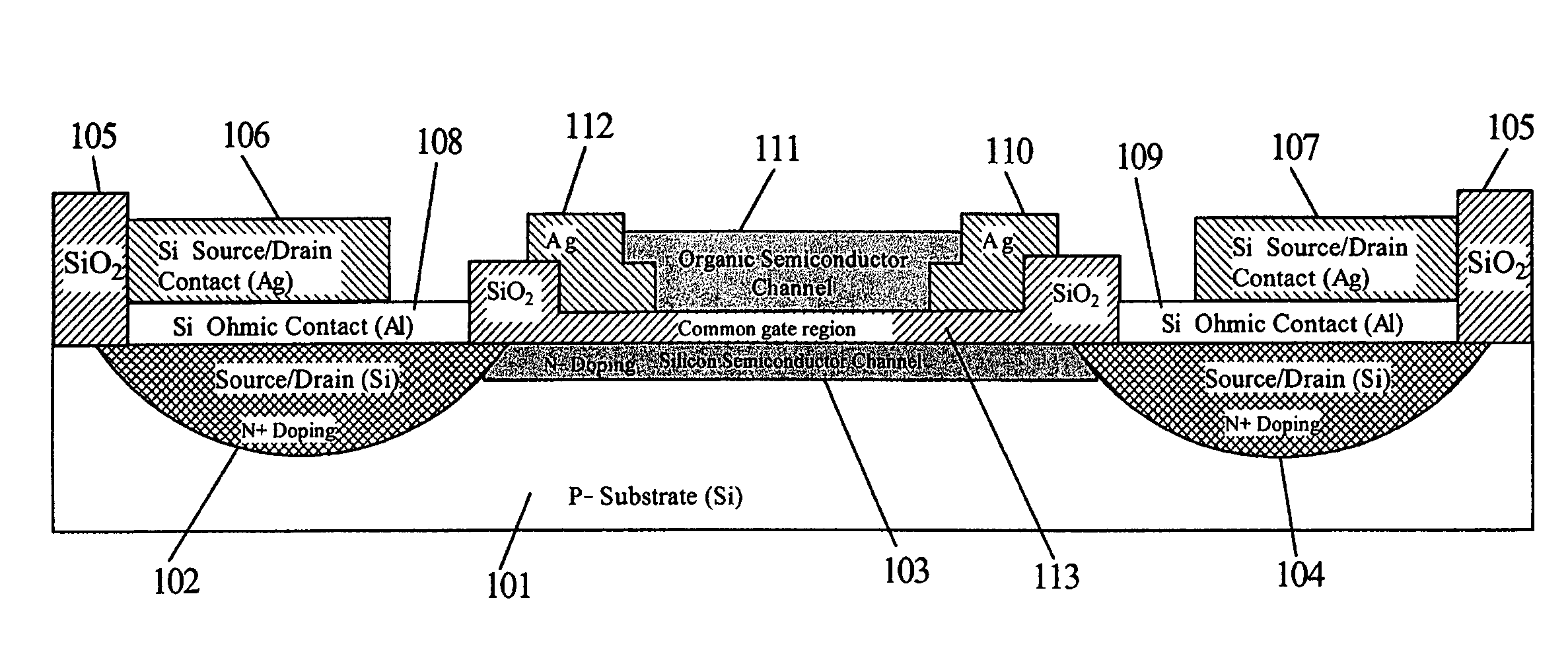
[0019]FIG. 1 is a cross-section view of a combination hybrid organic and silicon semiconductor FET device 100 according to embodiments of the present invention. The first step in device fabrication is to fabricate a silicon N-channel field effect transistor (NFET). Using photolithography and ion-implantation techniques, source 102 and drain 104 regions are patterned and doped with phosphorous in a P-type silicon substrate 101 (resistiv...


PUM


Abstract

A four terminal field effect device comprises a silicon field effect device with a silicon N-type semiconductor channel and an N+ source and drain region. An insulator is deposited over the N-type semiconductor channel. An organic semiconductor material is deposited over the insulator gate forming a organic semiconductor channel and is exposed to the ambient environment. Drain and source electrodes are deposited and electrically couple to respective ends of the organic semiconductor channel. The two independent source electrodes and the two independent drain electrodes form the four terminals of the new field effect device. The organic semiconductor channel may be charged and discharged electrically and have its charge modified in response to chemicals in the ambient environment. The conductivity of silicon semiconductor channel is modulated by induced charges in the common gate in response to charges in the organic semiconductor channel.

Description

TECHNICAL FIELD[0001]The present invention relates to hybrid composite silicon / organic field effect devices wherein the gate charge is induced by electrical as well as environmental elements.BACKGROUND INFORMATION[0002]The use of gas sensors and sensor arrays for odor analysis has attracted a great deal of attention in recent years. The principal goal of such research is to create a technology that can detect a wide range of odors with sufficient reproducibility, selectively, and stability to enable the construction of electronic noses that possess learning, storage, and recognition capabilities. Such systems are expected to be useful in a number of applications including food processing, environmental remediation, agriculture, and medical diagnostics. Organic transistors are being investigated for use in low cost flexible circuitry and in displays. It has been shown that organic transistors also make excellent gas sensors. The sensitivity of some organic transistors and a few gases...

Claims


Application Information

Patent Timeline
Patent Type & Authority Patents(United States)
IPC IPC(8): H01L27/28
CPCB82Y10/00B82Y15/00B82Y30/00H01L27/286G01N27/4141H01L2924/0002H01L2924/00H10K19/20
Inventor DODABALAPUR, ANANTHSHARMA, DEEPAKFINE, DANIEL
Owner BOARD OF RGT THE UNIV OF TEXAS SYST
Why Eureka
Try Eureka