Doped organic semiconductor materials and process for their preparation

a technology of organic semiconductor materials and semiconductor materials, applied in the direction of sustainable manufacturing/processing, final product manufacturing, and fluid protection, can solve the problems of limited sublimation ability of pyronine b chloride, low chemical stability, and difficult access, and achieve high luminescence quantum yield and quantum efficiency high. the effect of light yield

Active Publication Date: 2005-03-24
NOVALED GMBH
View PDF2 Cites 101 Cited by
  • Summary
  • Abstract
  • Description
  • Claims
  • Application Information

AI Technical Summary

Benefits of technology

[0012] Hence, the object of the present invention is to improve the preparation of organic doped semiconductor materials with respect to yield and purity.
[0013] In accordance with the invention, this object is achieved by using a neutral organic compound as dopant. By using the hydrogenated form of an organic compound in contrast to the direct use of a salt of the organic compound, the polymerization problems and the action of by-products—such as, e.g., hydrogen chloride—are avoided.
[0015] More expediently, the dopant in the hydrogenated form of the organic compound is prepared by subliming a salt of the organic compound. Thus, the preparation of the hydrogenated form of the organic compound is a prior independent step in the absence of the organic semiconductor material. Moreover, further purification processes can be carried out to improve the yield and purity of the hydrogenated form of the organic compound.
[0019] More advantageously, the uncharged organic compound is the carbinol base or leuco base of a cationic dye. Use of such molecules shows a high quantum efficiency of the light yield of organic light-emitting diodes. For example, cationic dyes, such as, e.g., rhodamine B, often have a high luminescence quantum yield, which permits later use as luminescence dyes in organic LED.

Problems solved by technology

The use of organic dopants is disadvantageous in that the desired doping materials, which are distinguished by extreme electron affinities or reduction potentials for p-doping or corresponding ionization potentials or oxidation potentials for n-doping, have a low chemical stability and are difficultly accessible.
A drawback of this process is due to the reaction to form the leuco form of the cationic dye.
In this reaction, polymerization of pyronine B takes place, which results in an only limited sublimability of pyronine B chloride.
This process is disadvantageous in so far as its use in vacuo is not possible and hence it cannot be used in combination with the usual organic semiconductor materials, such as, e.g., fullerene C60.
In principle, there is a direct reciprocal relationship between the stability of the dimer and that of the cation monomer, so that a cation monomer that is all the more stable is, as uncharged dimer, only of limited stability.

Method used


Image

  • Doped organic semiconductor materials and process for their preparation
  • Doped organic semiconductor materials and process for their preparation

Examples


Embodiment Construction

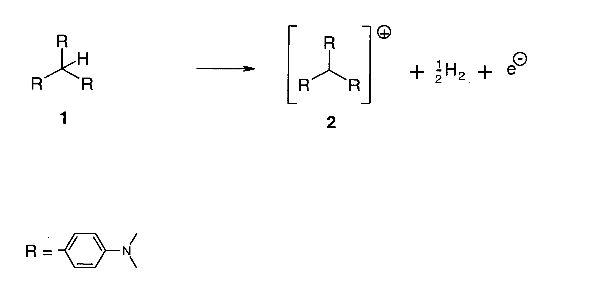
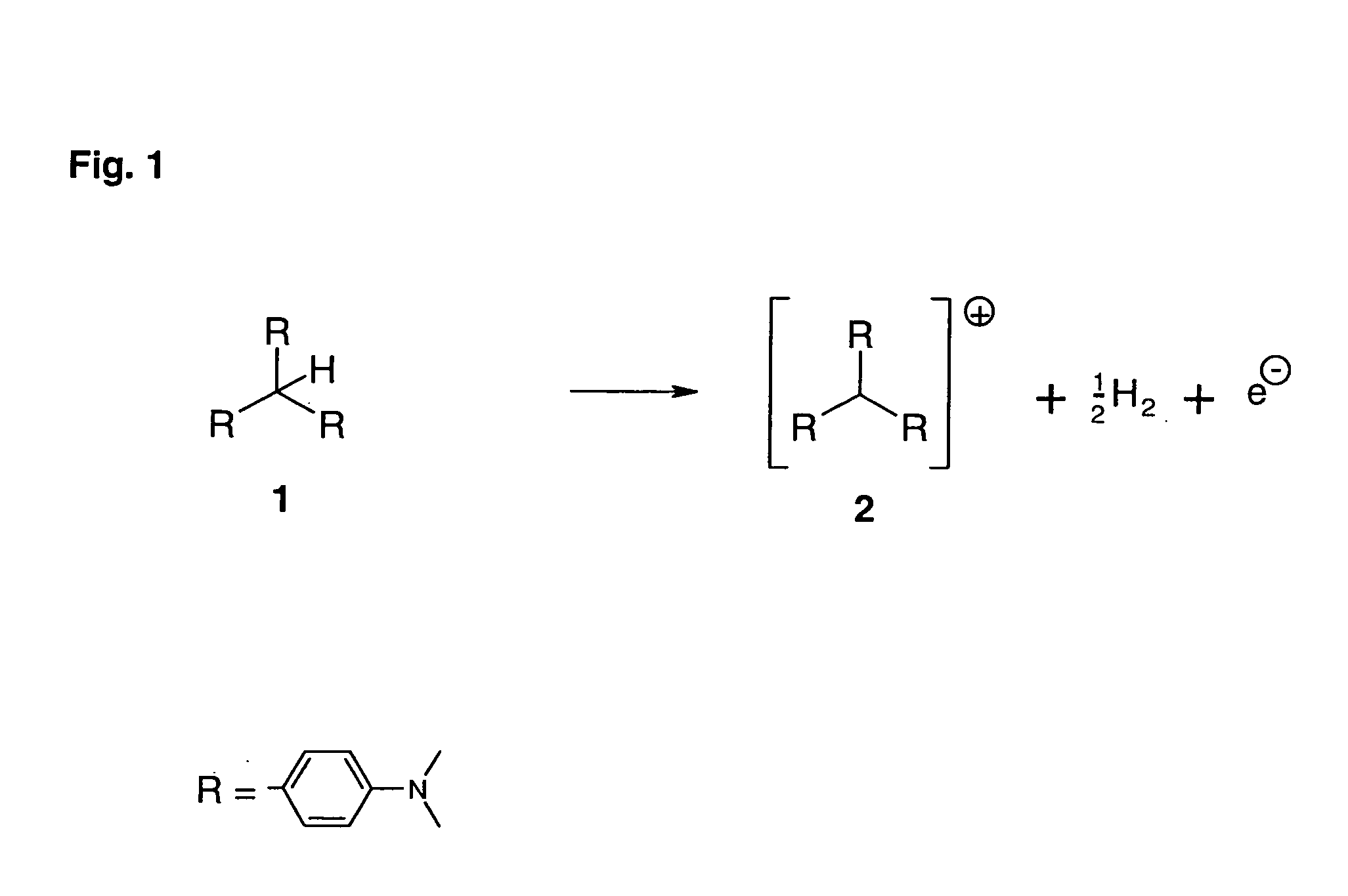
[0026] In an embodiment of the process of the invention to prepare doped organic semiconductors, Crystal Violet is used as cationic dye.

[0027] In a first step, the dye, present as the chloride salt and hence stable, is first sublimed. In this step, hydrogen chloride is liberated. The uncharged reduced form of Crystal Violet is obtained as its leuco base 1 in a small yield.

[0028] The leuco base 1 is a precursor substance, from which the donor 2 is obtained in a second step. In the absence of UV radiation, the Leuco Crystal Violet 1 is stable in air. Leuco Crystal Violet 2 has an oxidation potential of 0.7 V against SCE. In general, materials having oxidation potentials of more than 0.3 V against SCE are kinetically stable, i.e., they are inert in air. The inertness of Leuco Crystal Violet 1 in air has a direct advantageous effect on the simplicity of handling the precursor substance of the donor. Thus, the leuco base can be used directly in the doping process.

[0029] For this purpo...


PUM

PropertyMeasurementUnit
reduction potentialaaaaaaaaaa
reduction potentialsaaaaaaaaaa
charge carrier densityaaaaaaaaaa

Abstract

The present invention relates to a process for the preparation of doped organic semiconductor materials having an increased charge carrier density and effective charge carrier mobility, by doping with a dopant, a process in which after mixing the dopant into the organic semiconductor material, hydrogen, carbon monoxide, nitrogen or hydroxyl radicals are split off and at least one electron is transferred to the semiconductor material or from the semiconductor material. The process is distinguished by the fact that an uncharged organic compound is used as dopant. Doped organic semiconductor materials are obtainable by one of the processes. The semiconductor materials are distinguished by the fact that the doped layer contains cations of at least one organic compound, the uncharged form of the organic compound being unstable in air.

Description

CROSS-REFERENCE TO RELATED APPLICATIONS [0001] The present application claims priority to German Patent Application No. 103 38 406.5, filed Aug. 18, 2003, which is incorporated herein by reference in its entirety. BACKGROUND OF THE INVENTION [0002] The present invention relates to doped organic semiconductor materials having an increased charge carrier density and effective charge carrier mobility, as well as to a process for preparing them by doping with a dopant, wherein, after mixing the dopant into the organic semiconductor material, hydrogen, carbon monoxide, nitrogen or hydroxy radicals are split off and at least one electron is transferred to the semiconductor material or from the semiconductor material. [0003] Since the demonstration of organic light-emitting diodes and solar cells in 1989 (C. W. Tang et al., Appl. Phys. Lett., 1987, 913), components constructed from thin organic layers have been the subject of intensive research. Such layers have advantageous properties for...

Claims


Application Information

Patent Timeline
Patent Type & Authority Applications(United States)
IPC IPC(8): C07C13/15C07C13/24C07C15/20C30B15/00C30B21/06C30B23/00C30B25/00C30B27/02C30B28/10C30B28/12H01L51/50C30B28/14C30B30/04C30B31/00H01L31/04H01L51/00H01L51/30H01L51/40H01L51/42H05B33/14H05B33/22
CPCH01L51/002H01L51/005H01L51/0052Y02E10/549H01L51/0062H01L51/5052H01L51/0053Y02P70/50H10K71/30H10K85/60H10K85/621H10K85/649H10K85/615H10K50/155H10K50/165H10K99/00H10K10/00
Inventor WERNER, ANSGARLI, FENGHONGPFEIFFER, MARTIN
Owner NOVALED GMBH
Why Eureka
Try Eureka