

Organic field effect transistor with an organic dielectric
a dielectric transistor and organic field technology, applied in transistors, thermoelectric devices, solid-state devices, etc., can solve the problems of large influence on the performance of the transistor, /or cost, and difficulty in large-area application of techniques
Inactive Publication Date: 2006-04-18
MERCK PATENT GMBH
View PDF26 Cites 98 Cited by
- Summary
- Abstract
- Description
- Claims
- Application Information
AI Technical Summary
Benefits of technology
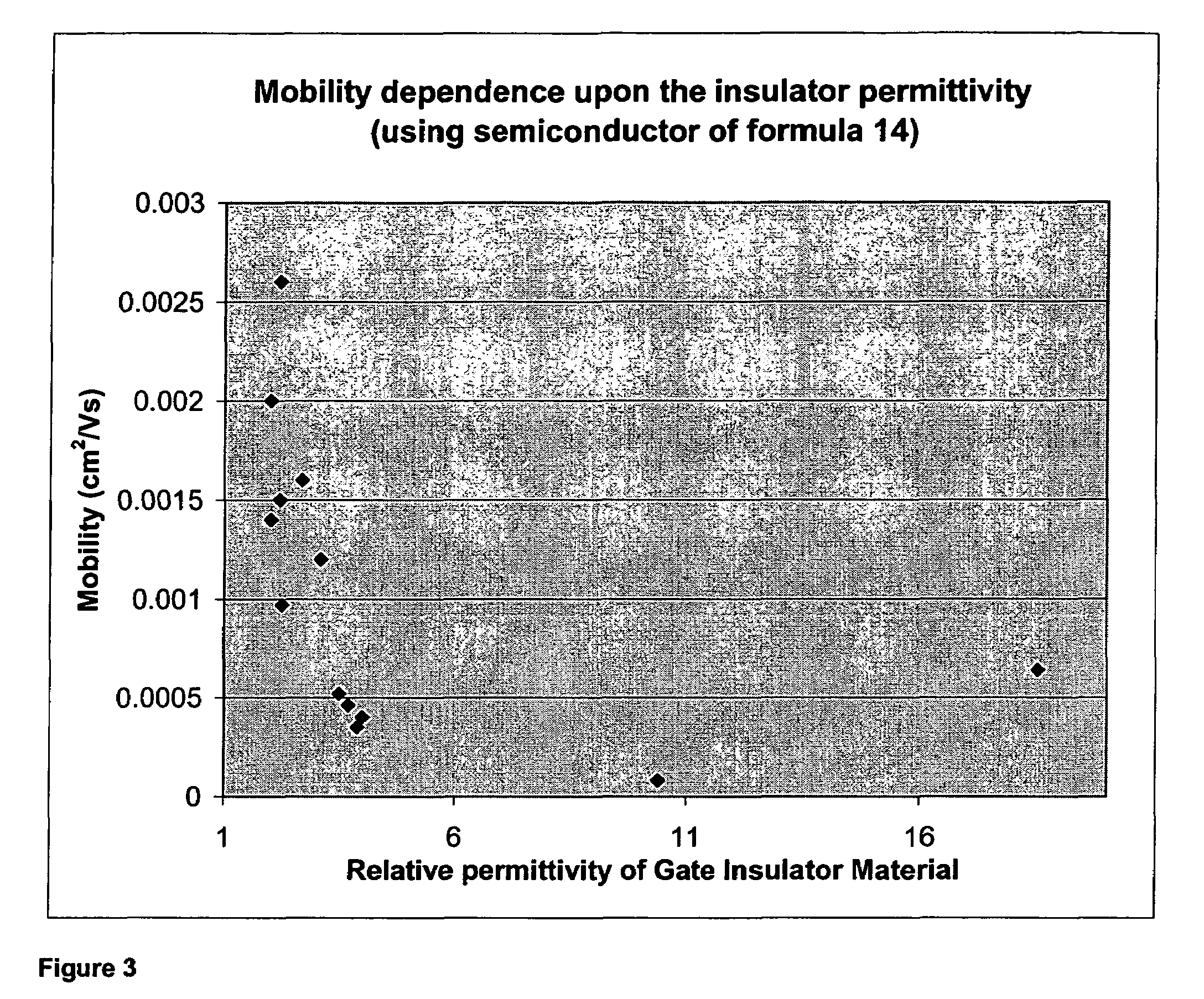
This approach results in organic field effect transistors with enhanced mobility and reproducibility, reduced dependence on gate field, and lower operating voltage, while maintaining a sharp interface between the semiconductor and insulator, thus overcoming the limitations of previous high permittivity insulator-based technologies.
Problems solved by technology
However, transistor performance is vastly affected by other components / materials used in an FET and also by the preparation conditions.
However, in order to achieve the orientation of the semiconductor layer, production processes have been used which are difficult and / or costly to apply to large areas, thus detracting from one of the potential advantages of OFETs, i.e. the possibility of solution coating the layers over large areas.
This orientation layer is not solution coated thus the technique is difficult to apply on large areas.
In addition as the PTFE is not in solution form the method is difficult to apply on large areas.
This makes the process incompatible with plastic substrates such as polyethylenenaphthalate or polyethyleneterephthalate and therefore is not preferred.
Vapour deposition of the OSC is also not preferred as it is difficult to apply on large areas.
Method used
View moreImage
Smart ImageViewing Examples

Examples
example 1
[0087]
This material was prepared using the procedure described in PCT / GB01 / 05145 to yield a yellow powder (7.8 g). Mw=3700.
example 2
[0088]
[0089]This material was prepared using the procedure described in PCT / GB01 / 05145 to yield a series of 13 fractions ranging from Mw=700 to Mw=10000.
example 3
[0090]
[0091]This material was prepared using the procedure described in WO 99 / 32537 to yield an off-white solid (20.2 g).(Mw=3100).
Login to View More PUM
| Property | Measurement | Unit |
|---|---|---|
| relative permittivity | aaaaa | aaaaa |
| relative permittivity | aaaaa | aaaaa |
| thickness | aaaaa | aaaaa |
Abstract
A process of manufacturing an organic field effect device is provided comprising the steps of (a) depositing from a solution an organic semiconductor layer; and (b) depositing from a solution a layer of low permittivity insulating material forming at least a part of a gate insulator, such that the low permittivity insulating material is in contact with the organic semiconductor layer, wherein the low permittivity insulating material is of relative permittivity from 1.1 to below 3.0. In addition, an organic field effect device manufactured by the process is provided.
Description
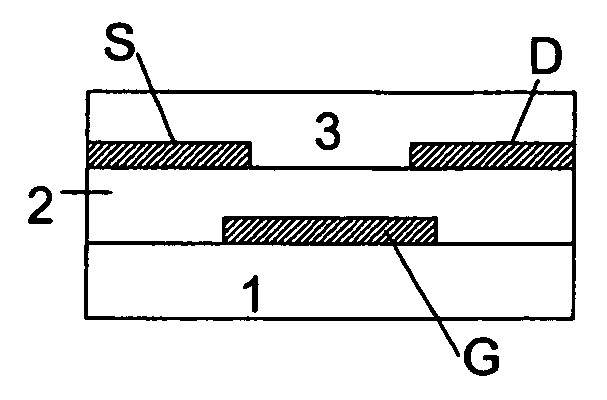
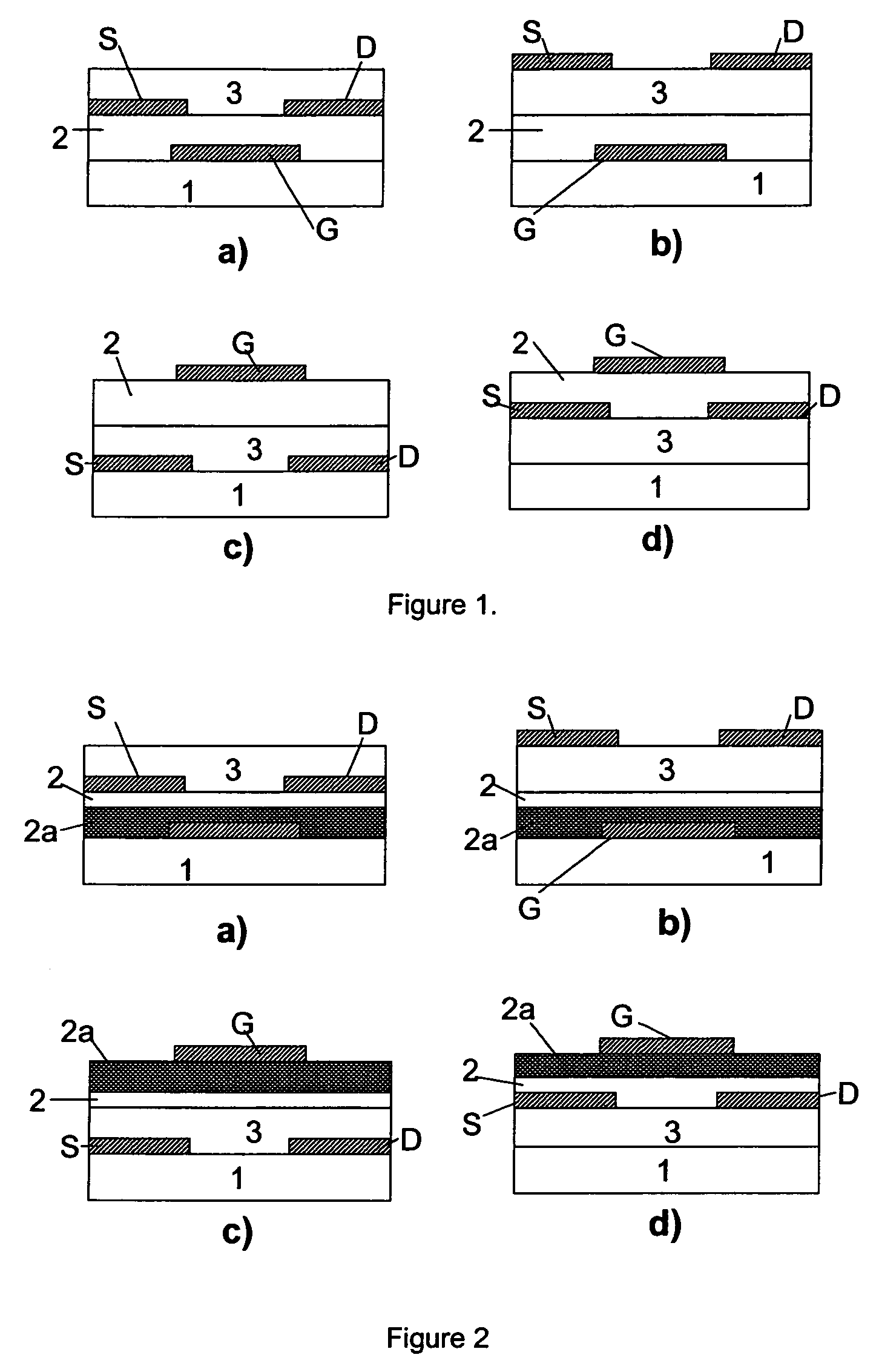
BACKGROUND OF THE INVENTION[0001]This invention relates to organic field effect transistors (OFETS) and processes for their manufacture.[0002]Field effect transistors (FET) based on inorganic materials such as Si are well established in the microelectronics industry. A typical FET consists of a number of layers and they can be configured in various ways. For example, an FET may comprise a substrate, an insulator, a semiconductor, source and drain electrodes connected to the semiconductor and a gate electrode adjacent the insulator. When a potential is applied on the gate electrode, charge carriers are accumulated in the semiconductor at its interface with the insulator. As a result, a conductive channel is formed between the source and the drain and a current will flow if a potential is applied to the drain.[0003]In the past decade there has been growing interest in developing FETs using organic materials. Organic devices offer the advantage of structural flexibility, potentially mu...
Claims
Login to View More Application Information
Patent Timeline
 Patent Type & AuthorityPatents(United States)
IPC IPC(8): H01L35/24H01L51/00H01L21/368H10N10/856H01L21/02H01L21/312H01L21/336H01L29/786H01L51/05H01L51/30H01L51/40
CPCH01L21/02282H01L51/052H01L51/0533C09B57/008C09B69/109H01L21/02118H01L21/0212C08G2261/11C08G2261/3142C08G2261/3162C08G2261/3223C08G2261/92H01L21/312H01L21/3127H01L28/56H01L51/0035H01L51/0036H01L51/0037H01L51/0039H01L51/0043H01L51/0052H01L51/0059H01L51/0541H01L51/0545C08G2261/12H01L21/02183H01L21/02186H10K85/115H10K85/111H10K85/1135H10K85/151H10K85/113H10K85/631H10K85/615H10K10/471H10K10/476H10K10/464H10K10/466
InventorVERES, JANOSOGIER, SIMON DOMINICMOHIALDIN-KHAFFAF, SOADLEEMING, STEPHEN WILLIAM
OwnerMERCK PATENT GMBH