

Organic Semiconducting Materials and Organic Component
a technology of organic components and semiconducting materials, which is applied in the direction of organic chemistry, basic electric elements, thermoelectric devices, etc., can solve the problems of undesired irregularities in electronic components, high control- and regulating costs within processes, and undesired ageing effects of electronic components
- Summary
- Abstract
- Description
- Claims
- Application Information
AI Technical Summary
Benefits of technology
Problems solved by technology
Method used
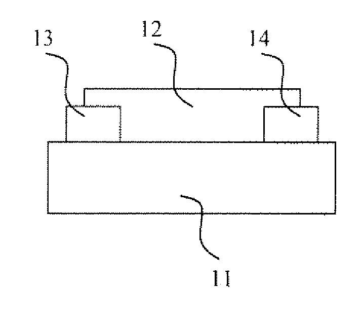
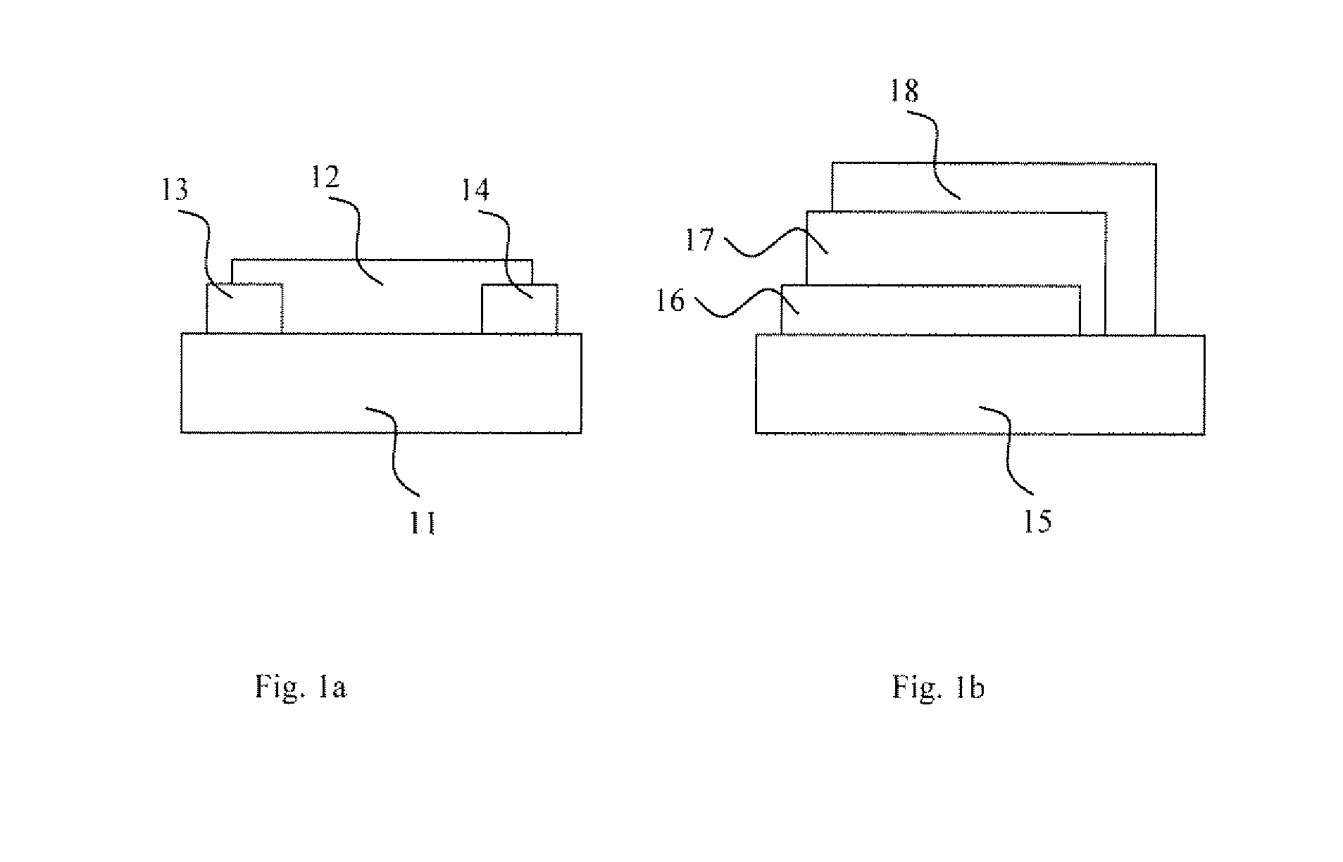
Image

Examples
Embodiment Construction
:
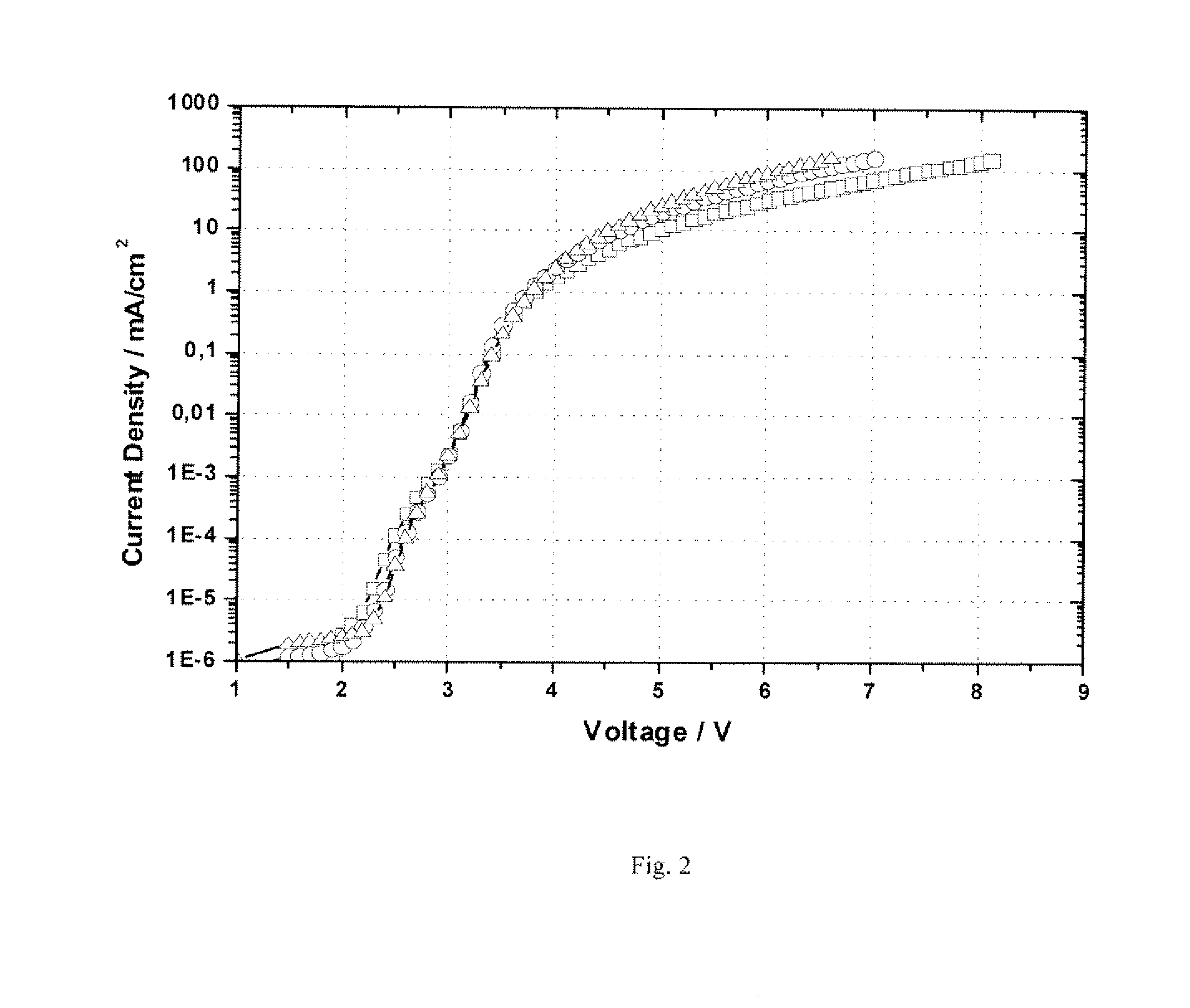
[0084]A 50 nm thick layer of HTM having formula 1 was doped with compound (p). The doped layer was produced by mixed evaporation of the HTM having formula 1 and dopant (p) in a high vacuum. The concentration of the doping agent in the matrix was 10 mmol %.
[0085]For HTM1, the following results were obtained: The vaporisation temperature of the doping agent was 170° C. The vaporisation temperature of the HTM1 was 288° C. The doped layer had a high conductivity of 1.58.10-4 S / cm. The layer had a thermal stability temperature of 110° C.
[0086]For HTM2, the following results were obtained: The vaporisation temperature of the doping agent was 163° C. The vaporisation temperature of the HTM2 was 279° C. The doped layer had a high conductivity of 2.45.10-4 S / cm. The layer had a thermal stability temperature of 108° C.
[0087]As a comparison, the following results were obtained for n=0 (a-NPD): The vaporisation temperature of the doping agent was 172° C. The vaporisation temperature of the □-N...
PUM
| Property | Measurement | Unit |
|---|---|---|
| Electric potential / voltage | aaaaa | aaaaa |
| Electric potential / voltage | aaaaa | aaaaa |
| Semiconductor properties | aaaaa | aaaaa |
Abstract
Description
Claims
Application Information