Folding chip planar stack package

a technology of stacking and chips, applied in the field of stacking chips, can solve the problems of increasing the manufacturing cost of the substrate, increasing the manufacturing cost of the boc type fbga package, and difficulty in increasing the capacity of the boc type fbga package, and achieve the effect of reducing the manufacturing cost of the substra

Inactive Publication Date: 2008-07-08
SK HYNIX INC
View PDF23 Cites 8 Cited by
  • Summary
  • Abstract
  • Description
  • Claims
  • Application Information

AI Technical Summary

Benefits of technology

[0010]Accordingly, an object of the present invention is to provide a folding chip planar stack package including a substrate, which has no window, thereby reducing the manufacturing cost thereof.
[0011]Another object of the present invention is to provide a folding chip planar stack package having a planar stack structure capable of ensuring superior signal transmission characteristics.
[0012]Still another object of the present invention is to provide a folding chip planar stack package having a planar stack structure realized by employing folding chips such that the size of the folding chip planar stack package can be reduced.
[0013]Still yet another object of the present invention is to provide a folding chip planar stack package having a planar stack structure, capable of minimizing the mounting space for the folding chip planar stack package.

Problems solved by technology

However, according to the above BOC type FBGA package, the window must be formed at the center portion of the substrate so as to wire-bond the bonding pad of the semiconductor chip to the bond finger of the substrate, so that the manufacturing cost for the substrate may increase as compared with that of the substrate, which does not require the window, thereby increasing the manufacturing cost for the BOC type FBGA package.
In addition, since only one semiconductor chip is accommodated in the BOC type FBGA package, it is difficult to increase the capacity of the BOC type FBGA package.
In addition, if bonding pads are aligned in a dual array structure, it is difficult to variously design the substrate relative to the stack, making it difficult to apply the semiconductor package to a high-speed product.
However, although the above planar stack package is suitable for edge pad type chips, it is not suitable for center pad type chips.
In addition, if the size of the semiconductor chip is enlarged, it is difficult to fabricate the planar stack package.
However, in this case, the mounting space for the planar stack package may be increased, so that the planar stack package has no practical use.
In addition, due to the limitation of the mounting space for the planar stack package, it may happen that fabrication of the planar stack package is impossible.

Method used


Image

  • Folding chip planar stack package
  • Folding chip planar stack package
  • Folding chip planar stack package

Examples


Embodiment Construction

[0026]Hereinafter, a preferred embodiment of the present invention will be described with reference to the accompanying drawings. In the following description and drawings, the same reference numerals are used to designate the same or similar components, so repetition of the description on the same or similar components will be omitted.

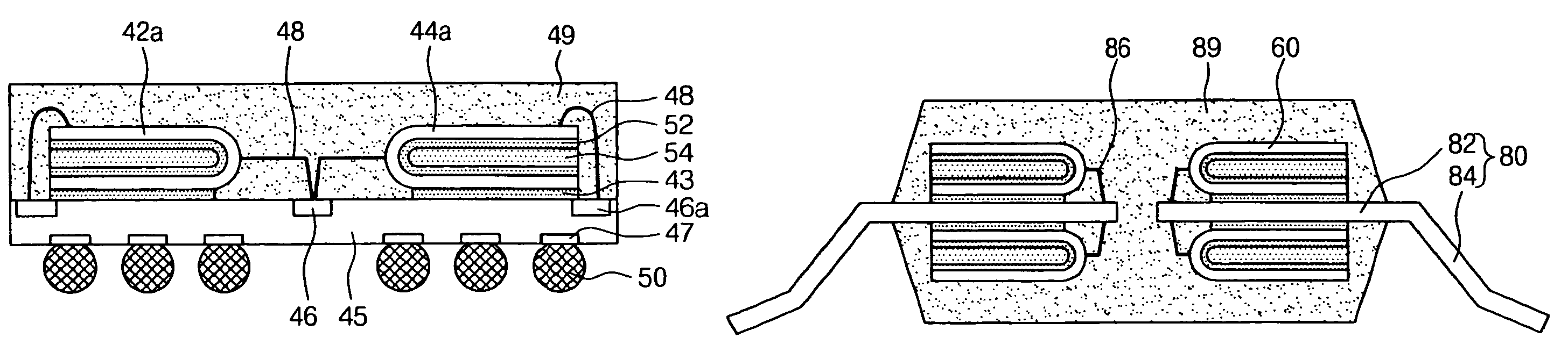
[0027]Referring now to FIG. 4 there is shown a sectional view of a folding chip planar stack package according to one embodiment of the present invention.

[0028]As shown in FIG. 4, the folding chip planar stack package includes a substrate 45, first and second semiconductor chips 42 and 44 attached to an upper surface of the substrate 45 while being spaced in parallel to each other, a plurality of bonding wires 48 for electrically connecting the first and second semiconductor chips 42 and 44 with the electrical contacts on or in the substrate 45, a sealing material 49 for sealing the upper surface of the substrate 45 including the first and second semi...


PUM


Abstract

A folding chip planar stack package is realized by employing folding chips. The folding chip planar stack package includes a substrate, first and second semiconductor chips attached to an upper surface of the substrate while being folded and spaced in parallel to each other, a bonding wire for electrically connecting the first and second semiconductor chips with the substrate, a sealing material for sealing the upper surface of the substrate including the first and second semiconductor chips and the bonding wire, and solder balls attached to a lower surface of the substrate.

Description

FIELD OF THE INVENTION[0001]The present invention relates to a stack package. More particularly, the present invention relates to a folding chip planar stack package obtained by folding semiconductor chips.BACKGROUND OF THE INVENTION[0002]As generally known in the art, semiconductor packages have been developed to have a compact size while improving various electrical characteristics thereof. A representative example of the semiconductor package is a so-called BGA (ball grid array) package. As is known to those of ordinary skill in the art, a BGA package has a size similar to that of a semiconductor chip, so that the mounting space for the BGA package can be minimized. In addition, since the BGA package is electrically connected to external circuits through one or more solder balls on the BGA package, the transmission path between the BGA package solder ball and a semiconductor chip inside the package is kept as short as possible, so that the electrical characteristics of the BGA pa...

Claims


Application Information

Patent Timeline
Patent Type & Authority Patents(United States)
IPC IPC(8): H01L23/02
CPCH01L23/3128H01L23/49575H01L23/5387H01L24/48H01L25/0655H01L29/0657H01L2224/0401H01L2224/05599H01L2224/32014H01L2224/48091H01L2224/48137H01L2224/48227H01L2224/4824H01L2224/48247H01L2224/484H01L2224/73215H01L2224/73265H01L2224/85399H01L2225/06579H01L2924/01002H01L2924/01004H01L2924/01082H01L2924/014H01L2924/15311H01L2924/00014H01L2924/01006H01L2924/01033H01L2224/32145H01L2224/32225H01L2224/32245H01L2224/06135H01L2224/06136H01L2224/45099H01L2924/00H01L2924/00012H01L2924/181H01L24/73H02H3/04H01H71/123
Inventor LEE, IK JAE
Owner SK HYNIX INC
Why Eureka
Try Eureka