Test structure and probe for differential signals

a technology of differential signals and probes, applied in the field of probes and test structures for differential signals, can solve the problems of affecting the accuracy of testing, electrically, and noise from external sources such as adjacent conductors, and affecting the operation of differential devices

Inactive Publication Date: 2008-07-22
CASCADE MICROTECH
View PDF1183 Cites 42 Cited by
  • Summary
  • Abstract
  • Description
  • Claims
  • Application Information

AI Technical Summary

Problems solved by technology

In addition, noise from external sources, such as adjacent conductors, tends to couple, electrically and electromagnetically, in the common mode and cancel in the differential mode.
However, the impedance of the internal connections of the DUT's components are often frequency dependant complicating de-embedding of the DUT and affecting the accuracy of the testing.
As a result, input impedance of the differential device varies substantially with frequency, producing instability in the operation of the differential device.

Method used


Image

  • Test structure and probe for differential signals
  • Test structure and probe for differential signals
  • Test structure and probe for differential signals

Examples


Embodiment Construction

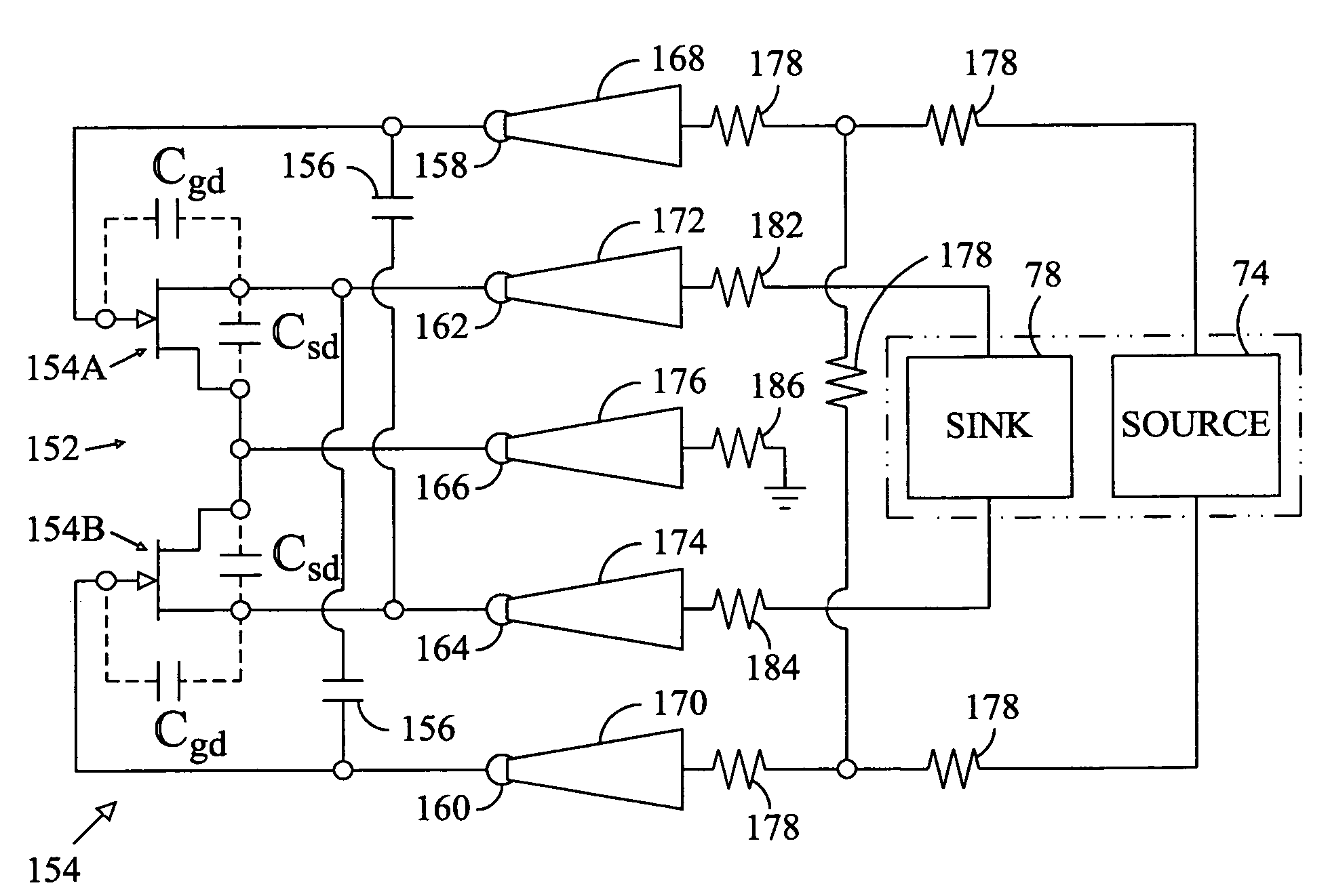
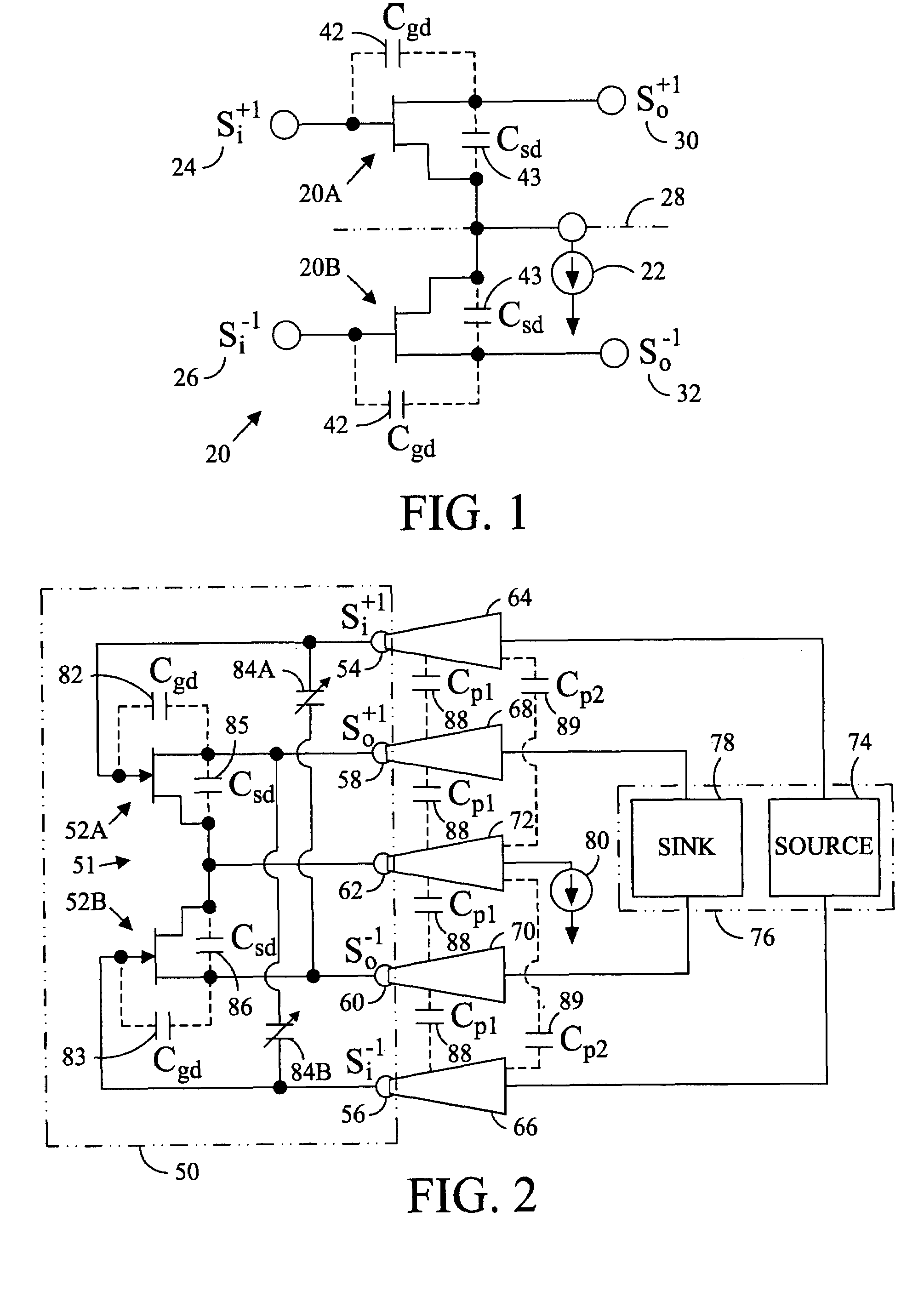
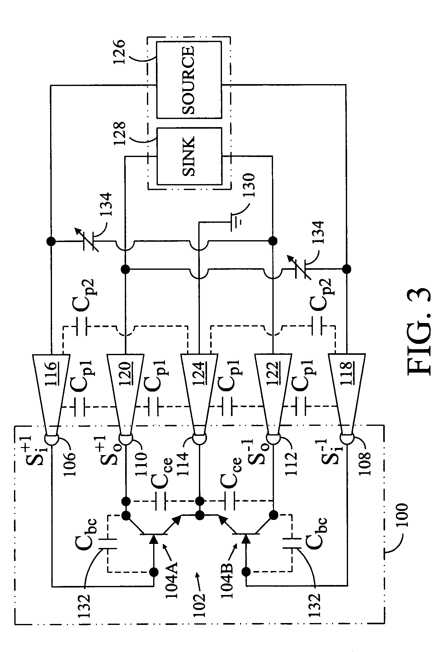
[0016]Referring in detail to the drawings where similar parts are identified by like reference numerals, and, more particularly to FIG. 1, a differential gain cell 20 is a balanced device comprising two nominally identical circuit halves 20A, 20B. When biased, with a DC current source 22, and stimulated with a differential mode signal, comprising even and odd mode components of equal amplitude and opposite phase (Si+1 and Si−1) 24, 26, a virtual ground is established at the symmetrical axis 28 of the two circuit halves. At the virtual ground, the potential at the operating frequency does not change with time regardless of the amplitude of the stimulating signal. The quality of the virtual ground of a balanced device is independent of the physical ground path and, therefore, balanced or differential circuits can tolerate poor RF grounding better than circuits operated with single ended (ground referenced) signals. Differential devices can also typically operate with lower signal powe...


PUM


Abstract

A test structure including a differential gain cell and a differential signal probe include compensation for the Miller effect reducing the frequency dependent variability of the input impedance of the test structure.

Description

CROSS-REFERENCE TO RELATED APPLICATIONS[0001]This application claims the benefit of U.S. Provisional App. No. 60 / 813,120, filed Jun. 12, 2006.BACKGROUND OF THE INVENTION[0002]The present invention relates to wafer probing and, more particularly, to probes and test structures for wafer probing with differential signals.[0003]Integrated circuits (ICs) are economically attractive because large numbers of often complex circuits, for example microprocessors, can be inexpensively fabricated on the surface of a wafer or substrate. Following fabrication, individual dies, including one or more circuits, are separated or singulated and encased in a package that provides for electrical connections between the exterior of the package and the circuit on the enclosed die. The separation and packaging of a die comprises a significant portion of the cost of manufacturing the integrated circuit device and to monitor and control the IC fabrication process and avoid the cost of packaging defective die...

Claims


Application Information

Patent Timeline
Patent Type & Authority Patents(United States)
IPC IPC(8): G01R31/02
CPCG01R31/2889
Inventor CAMPBELL, RICHARD
Owner CASCADE MICROTECH
Why Eureka
Try Eureka