Phase change memory device

a memory device and phase change technology, applied in the field of memory devices, can solve the problems of inability to meet the resistance of the writing circuit and/or the reading circuit to the selected phase change memory cell, affecting the operation of the phase change memory device, and affecting the operation of the digital storage devi

Active Publication Date: 2008-07-29
SAMSUNG ELECTRONICS CO LTD
View PDF14 Cites 17 Cited by
  • Summary
  • Abstract
  • Description
  • Claims
  • Application Information

AI Technical Summary

Problems solved by technology

This difference in length may affect the operation of the phase change memory device.
That is, because resistance exists on the individual global bit lines, resistance from the writing circuit and / or the reading circuit to the selected phase change memory cell may not be uniform.
These differences in resistance between phase change memory cells and reading / writing circuits may lead to undesirable consequences.
This difference in write current may lead to errors in the programming operations of phase change memory devices.

Method used


Image

  • Phase change memory device
  • Phase change memory device
  • Phase change memory device

Examples


Embodiment Construction

[0020]Features of the present invention and methods of accomplishing the same may be understood more readily by reference to the following detailed description of exemplary embodiments and the accompanying drawings. The present invention may, however, be embodied in many different forms and should not be construed as being limited to the embodiments set forth herein. Rather, these embodiments are provided so that this disclosure will be thorough and complete and will fully convey the concept of the invention to those skilled in the art, and the present invention will only be defined by the appended claims. Like reference numerals refer to like elements throughout the specification.

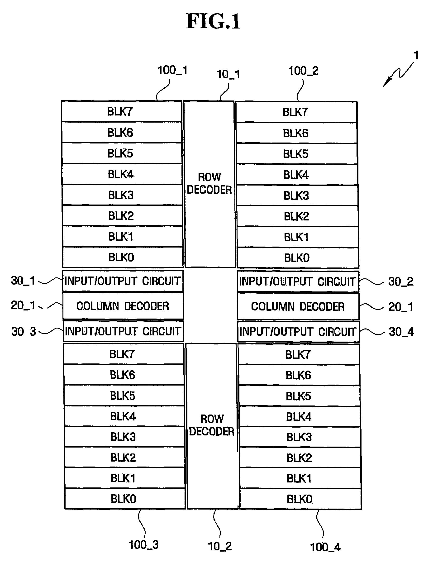
[0021]FIG. 1 is a block diagram illustrating a phase change memory device according to an exemplary embodiment. In FIG. 1, four memory banks are illustrated for convenience of explanation, but the present disclosure is not limited to this configuration.

[0022]Referring to FIG. 1, a phase change memory devic...


PUM


Abstract

A phase change memory device includes a semiconductor substrate which includes a plurality of phase change memory cells, a plurality of local bit lines extending over the semiconductor substrate, each of the plurality of local bit lines being coupled to the plurality of phase change memory cells, and a plurality of global bit lines extending over the plurality of local bit lines, each of the plurality of global bit lines being selectively coupled to the plurality of local bit lines. The plurality of global bit lines are located at two or more different wiring line levels over the semiconductor substrate.

Description

BACKGROUND OF THE INVENTION[0001]1. Field of the Invention[0002]The present disclosure relates generally to memory devices and, more particularly, the present invention relates to phase change memory devices.[0003]A claim of priority is made to Korean Patent Application No. 10-2006-003272, filed on Jan. 11, 2006, in the Korean Intellectual Property Office, the disclosure of which is incorporated herein by reference in its entirety.[0004]2. Description of the Related Art[0005]Phase change random access memory devices (PRAM) store data using a phase change material, such as, for example, a chalcogenide alloy, that transforms into a crystalline state or an amorphous state during cooling after heat treatment. Each state of the phase change material has different resistance characteristics. Specifically, the phase change material in the crystalline state has low resistance and the phase change material in the amorphous state has high resistance. The crystalline state is typically referre...

Claims


Application Information

Patent Timeline
Patent Type & Authority Patents(United States)
IPC IPC(8): G11C11/22
CPCG11C7/18G11C8/12G11C13/0004G11C2213/79G11C2213/72H10N70/231
Inventor CHOI, BYUNG-GILKIM, DU-EUNGCHO, WOO-YEONG
Owner SAMSUNG ELECTRONICS CO LTD
Why Eureka
Try Eureka