Output buffer circuit with control circuit for changing resistance of output resistor pair

a buffer circuit and output resistor technology, applied in pulse generators, pulse techniques, instruments, etc., can solve the problems of transmission line loss, waveform deterioration, and increase current consumption, so as to reduce jitter and increase current consumption

Inactive Publication Date: 2008-08-05
RENESAS ELECTRONICS CORP
View PDF11 Cites 30 Cited by
  • Summary
  • Abstract
  • Description
  • Claims
  • Application Information

AI Technical Summary

Benefits of technology

[0038]Meanwhile, there is disclosed in Patent Document 2 a configuration of an LVDS driver in which an edge of a pulse waveform in an input signal is detected and the current supplied to an output signal line through each switching device as from the so detected edge is increased for an extremely short time to improve the rise and fall characteristics and hence the frequency characteristics in the differential signal output to the output signal line.[Patent Document 1]
[0065]According to the present invention, the output resistors are variably controlled in association operatively with the operation of preemphasis, such that, when the preemphasis function is applied, the jitter may be diminished without increasing the current consumption.

Problems solved by technology

However, since a constant current source is needed, it is supposed that current consumption tends to be increased.
As a matter of fact, it is the power consumption which mainly determines the dominance of products by the different vendors.
The waveform of a transmission signal tends to deteriorate due to the increase of transmission speed and the increase of transmission distance.
With wide spread use of a broadband system and high speed transmission, waveform deterioration, ascribable to transmission line loss, as shown schematically in FIG. 2, is becoming of serious concern.

Method used


Image

  • Output buffer circuit with control circuit for changing resistance of output resistor pair
  • Output buffer circuit with control circuit for changing resistance of output resistor pair
  • Output buffer circuit with control circuit for changing resistance of output resistor pair

Examples


Embodiment Construction

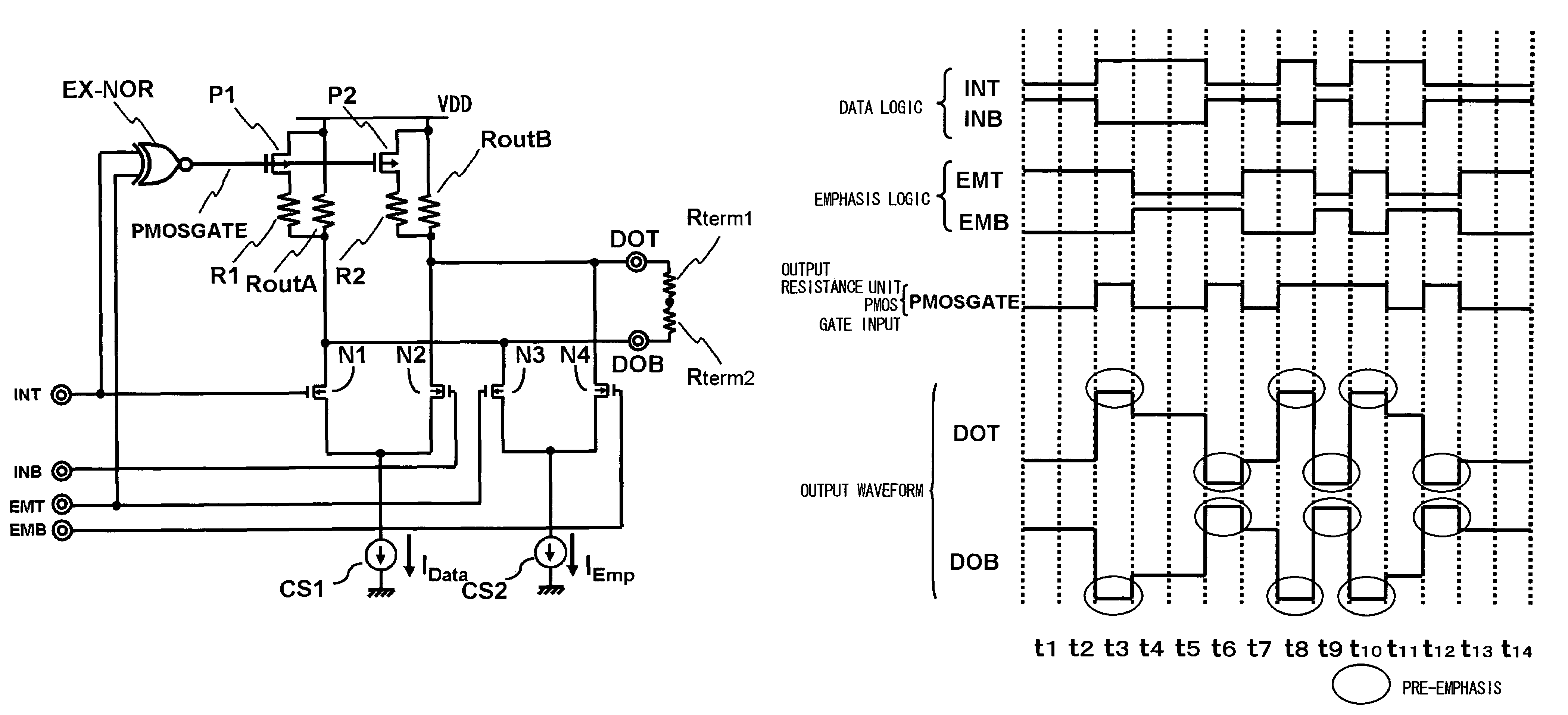
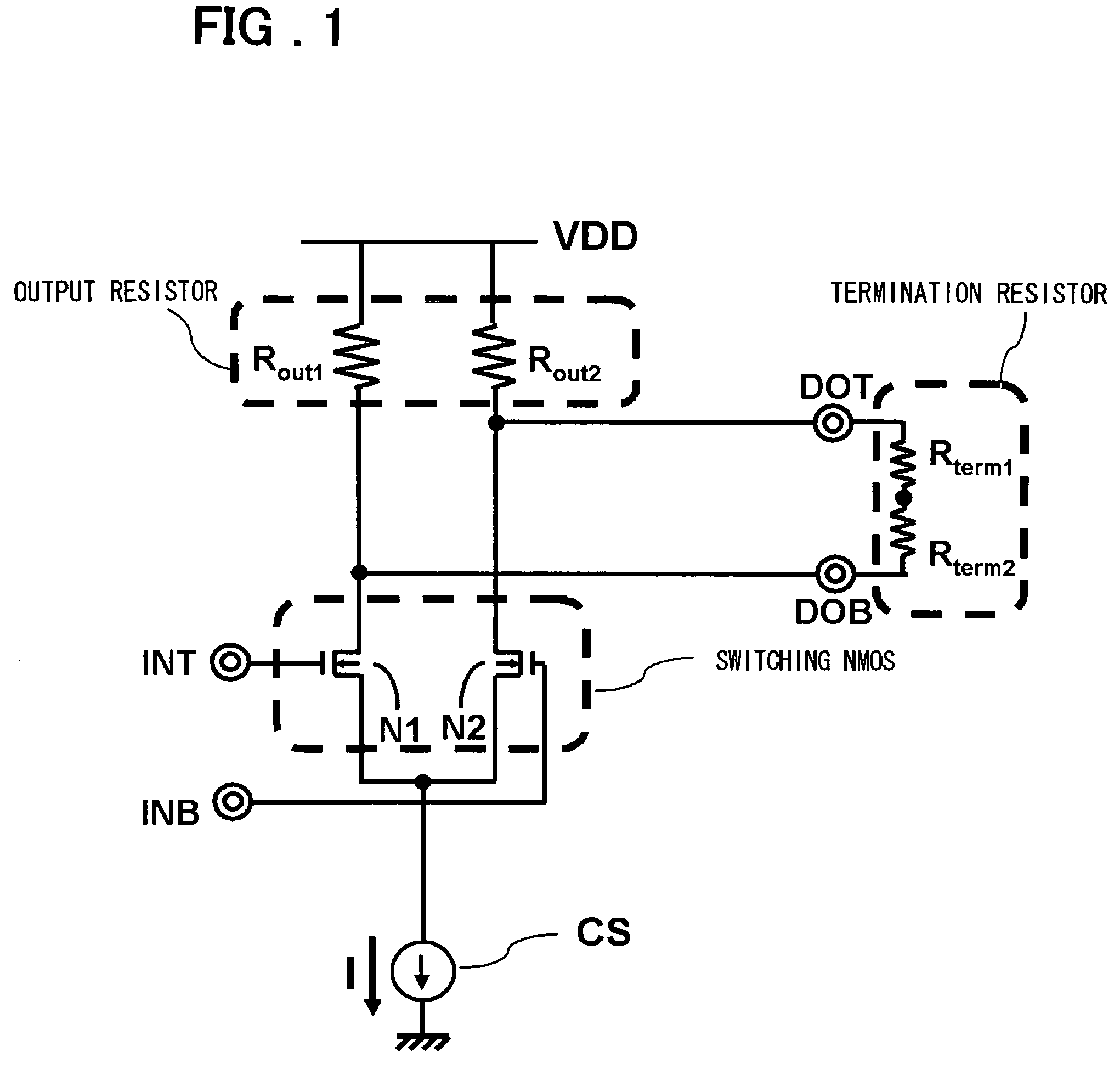
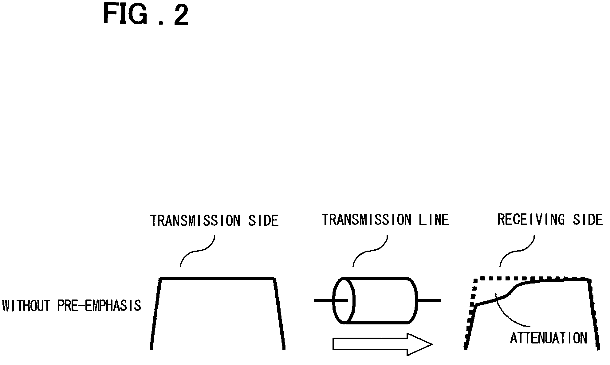
[0082]Referring to the drawings, the present invention will now be described in further detail. The output buffer circuit of the current mode logic, according to the present invention, includes an output resistor between an output pair of a differential circuit and a power supply and has a preemphasis function emphasizing the amplitude when the logic of an output signal undergoes a transition. The output buffer circuit performs switching control so that, at the time of preemphasis, the resistance value of the output resistor will be relatively larger. After the preemphasis, when the output signal is at the same logic as that to which the output signal has transitioned, deemphasis is performed for decreasing the amplitude emphasized. At this time, switching control is exercised so that the resistance value of the output resistor will become relatively smaller. More specifically, the output buffer circuit includes variable resistance elements (P1 and P2 of FIG. 9 and N1 and N2 of FIG....


PUM


Abstract

Disclosed is an output buffer circuit including a first differential transistor pair for differentially receiving a data signal from a differential input pair; and a second differential transistor pair for differentially receiving an emphasis data signal from another differential input pair; a pair of output resistor circuits via which the drains of first and second differential transistor pairs are connected to a power supply, said output resistor circuits each including a transistor; and a logic circuit adapted for receiving the data signal and the emphasis signal and for supplying a control signal which is of first and second values at the time of preemphasis and at other times to the transistors of the output resistor circuit, wherein the output resistance is relatively made larger at the time of emphasis, while being relatively smaller at the time of deemphasis.

Description

FIELD OF THE INVENTION[0001]This invention relates to an output buffer circuit for a semiconductor device. More particularly, this invention relates an output buffer circuit equipped with a preemphasis function.BACKGROUND OF THE INVENTION[0002]FIG. 1 is a diagram showing the configuration of a conventional CML (Current Mode Logic) driver circuit. The CML driver circuit includes N channel MOS transistors (NMOS transistors) N1 and N2, composing a differential circuit and constituting a switching device. The NMOS transistors N1 and N2 have coupled sources connected to a constant current source CS, have gates connected to differential input terminals INT and INB, respectively and have drains connected to a power supply VDD via output resistors Rout1 and Rout2. The drains of the NMOS transistors N1 and N2 are also connected to differential output terminals DOT and DOB, respectively. The differential output terminals DOT and DOB are connected to both ends of termination resistors Rterm1 a...

Claims


Application Information

Patent Timeline
Patent Type & Authority Patents(United States)
IPC IPC(8): H03K3/00
CPCH03K19/09432H03K19/018528
Inventor SUENAGA, SHUJI
Owner RENESAS ELECTRONICS CORP
Why Eureka
Try Eureka