System and method for designing and optimizing the memory of an embedded processing system

a technology of embedded processing and memory, applied in the field of memory design applications, can solve the problems of occupying the smallest amount of die space possible, and limiting the amount of embedded memory that will be available in the system

Inactive Publication Date: 2008-08-12
STMICROELECTRONICS SRL
View PDF3 Cites 40 Cited by
  • Summary
  • Abstract
  • Description
  • Claims
  • Application Information

AI Technical Summary

Benefits of technology

[0013]According to a still further embodiment of the present invention, the apparatus further comprises a code optimization controller capable of modifying the test program in response to the comparison of the memory usage statistical data and the one or more predetermined design criteria to thereby enable the embedded processing system to execute the test program according to the one or more predetermined design criteria.

Problems solved by technology

The demand for high-performance processing devices requires that state-of-the-art integrated circuits perform operations in the minimum amount of time, consume the minimum amount of power, and occupy the smallest amount of die space possible.
Circuit designers frequently make trade-offs when designing embedded processing systems.
One major issue that must be resolved when designing an ASIC device or other embedded processing system is the amount of embedded memory that will be available in the system.
Unfortunately, while modern design tools, such as compilers and debuggers, are capable of telling circuit designers the total amount of memory needed, they tell very little else about the memory requirements of an ASIC device.
The end result is that many ASIC devices run slower, consume more power, or are larger in size than would otherwise have been necessary.

Method used


Image

  • System and method for designing and optimizing the memory of an embedded processing system
  • System and method for designing and optimizing the memory of an embedded processing system
  • System and method for designing and optimizing the memory of an embedded processing system

Examples


Embodiment Construction

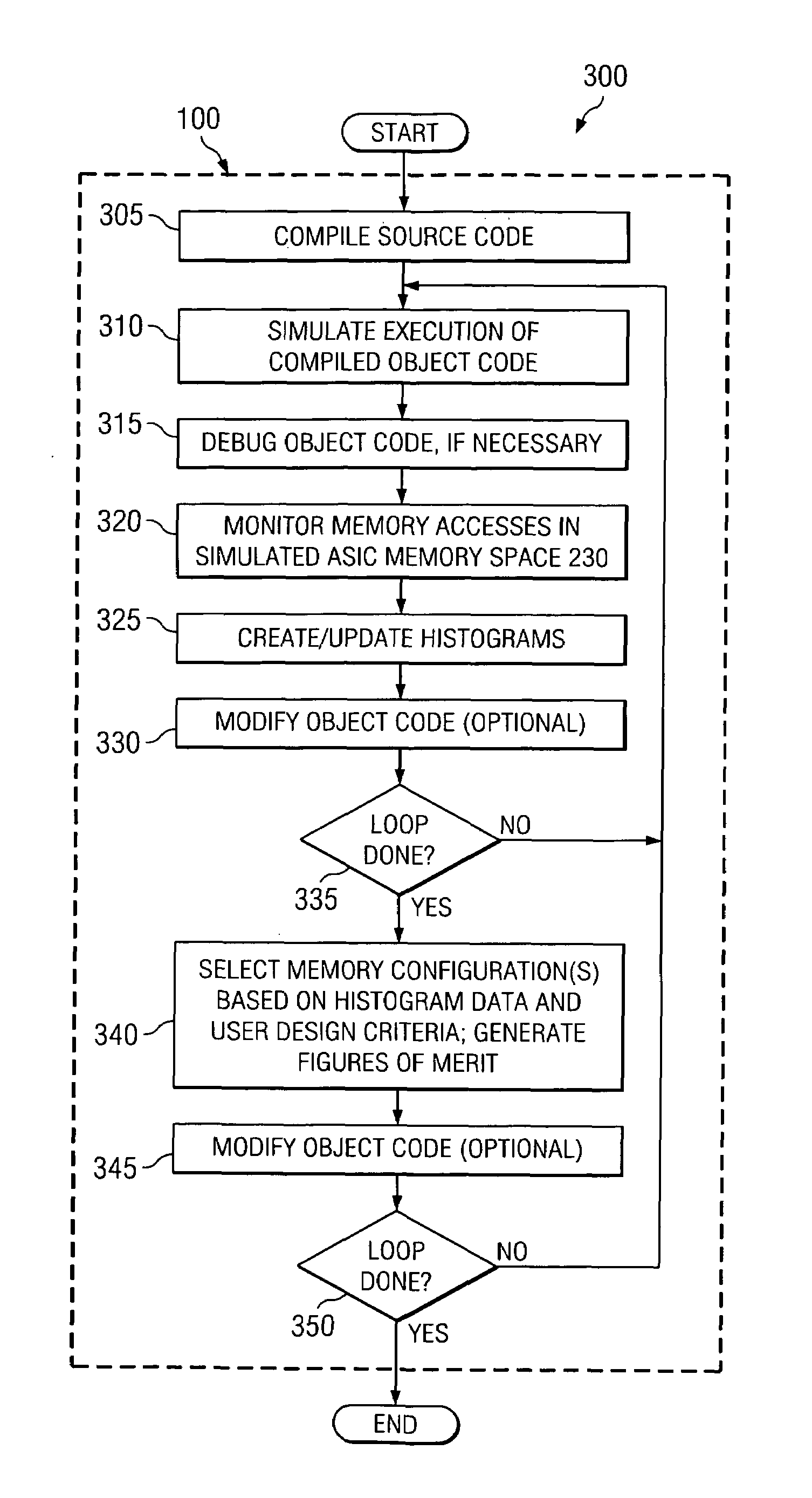
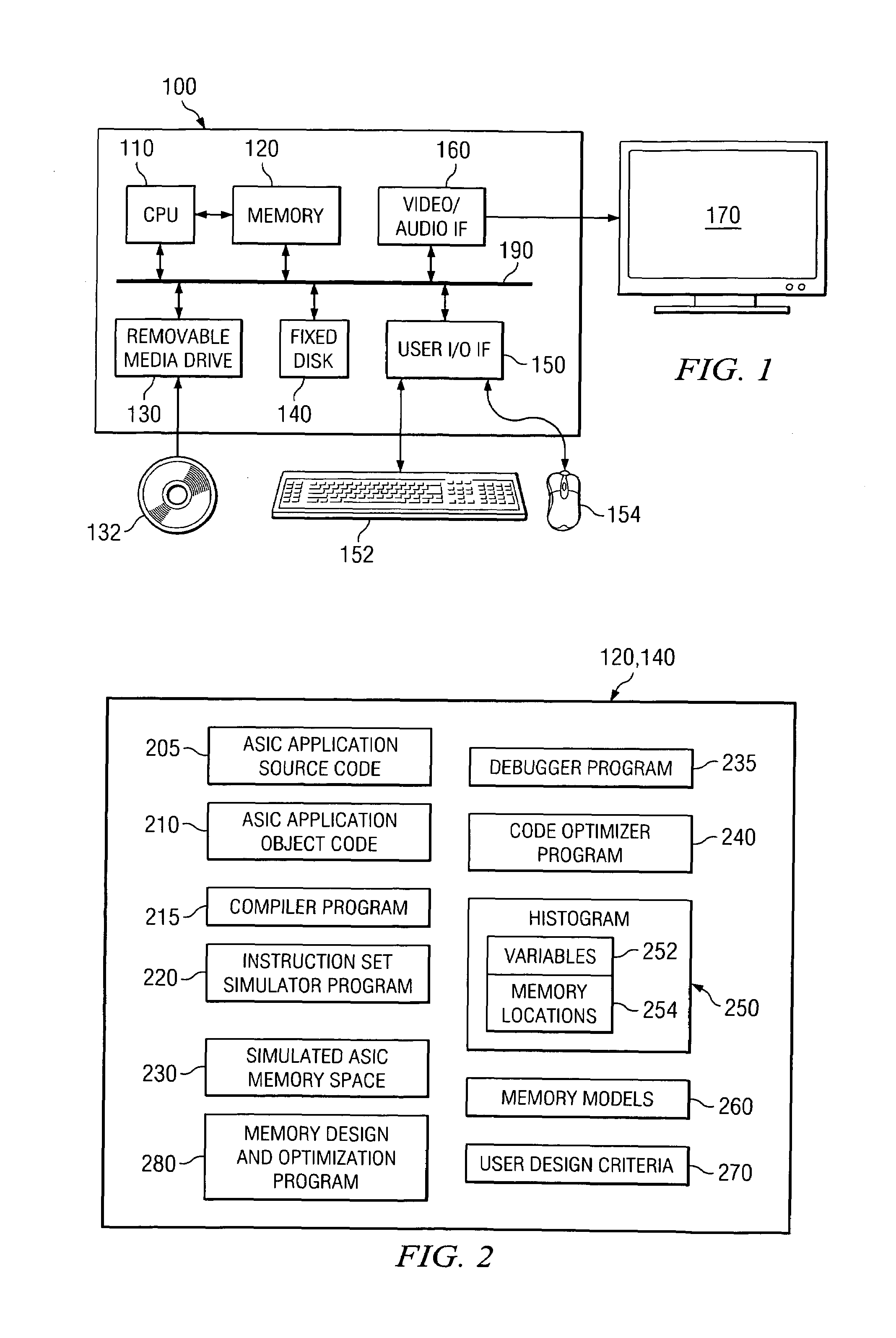
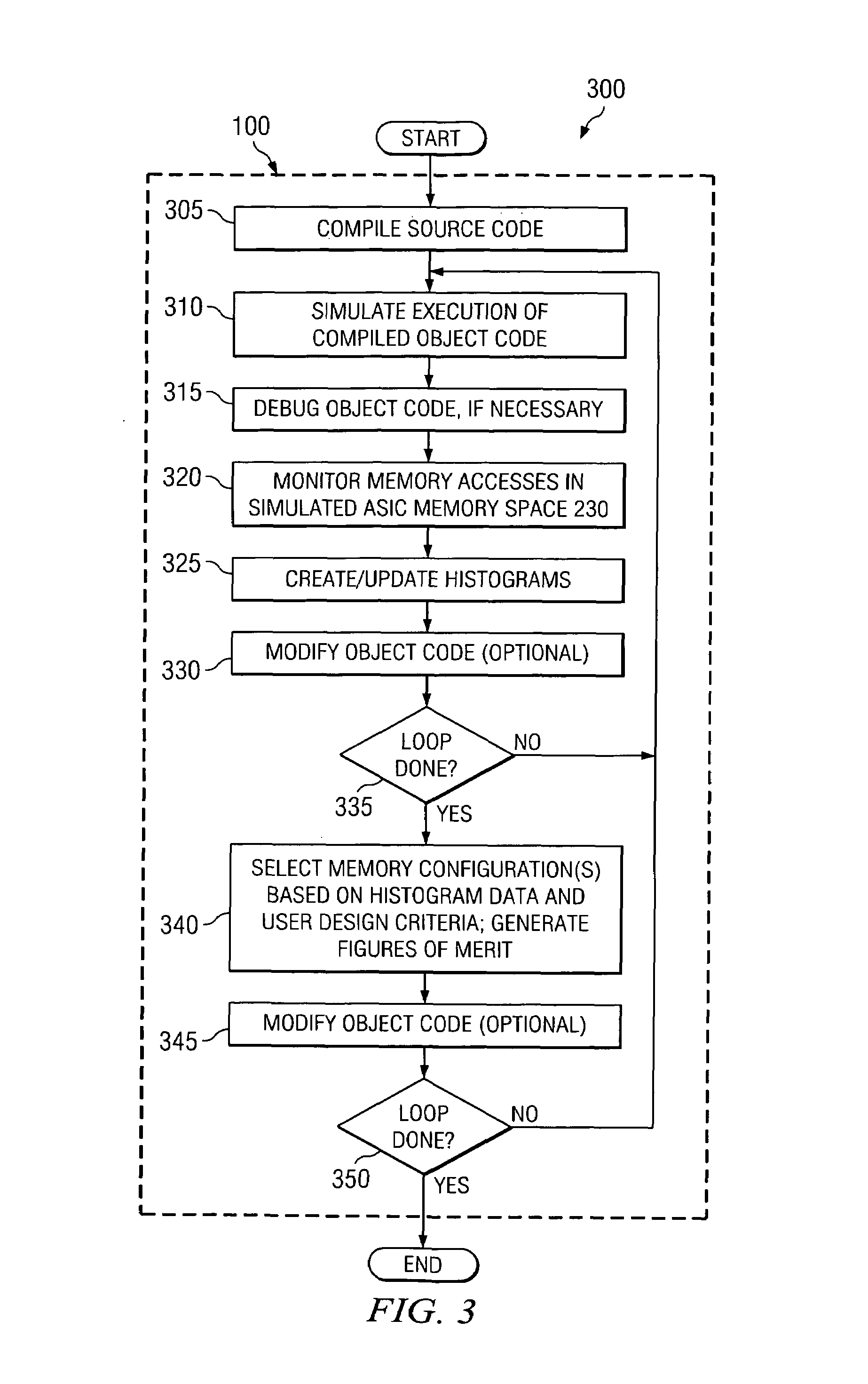
[0020]FIGS. 1 through 3, discussed below, and the various embodiments used to describe the principles of the present invention in this patent document are by way of illustration only and should not be construed in any way to limit the scope of the invention. Those skilled in the art will understand that the principles of the present invention may be implemented in any suitably arranged processing system.

[0021]FIG. 1 illustrates exemplary processing system 100, which is capable of designing and optimizing the memory of an embedded system, such as an application specific integrated circuit (ASIC), according to one embodiment of the present invention. In an advantageous embodiment, processing system 100 may be embodied in a personal computer (PC) or equivalent workstation (as shown in FIG. 1) that contains a processor and memory capable of executing memory design applications and / or memory optimization applications according the principles of the present invention.

[0022]Processing syst...


PUM


Abstract

There is disclosed an apparatus for designing and optimizing a memory for use in an embedded processing system. The apparatus comprises: 1) a simulation controller for simulating execution of a test program to be executed by the embedded processing system; 2) a memory access monitor for monitoring memory accesses to a simulated memory space during the simulated execution of the test program, wherein the memory access monitor generates memory usage statistical data associated with the monitored memory accesses; and 3) a memory optimization controller for comparing the memory usage statistical data and one or more predetermined design criteria associated with the embedded processing system and, in response to the comparison, determining at least one memory configuration capable of satisfying the one or more predetermined design criteria.

Description

TECHNICAL FIELD OF THE INVENTION[0001]The present invention is generally directed to memory design applications and, more specifically, to a system design tool capable of determining the memory access usage of an embedded processing system and selecting and optimizing the types and sizes of memories used in the embedded processing system.BACKGROUND OF THE INVENTION[0002]The demand for high-performance processing devices requires that state-of-the-art integrated circuits perform operations in the minimum amount of time, consume the minimum amount of power, and occupy the smallest amount of die space possible. This is particularly true of a wide array of embedded processing systems, such as application-specific integrated circuit (ASIC) devices, that contain a processor and memory. ASIC devices and other embedded processing systems are used in network cards, modems, wireless receivers and transmitters, smart cards, cell phones, personal digital assistant (PDA) devices, and the like.[0...

Claims


Application Information

Patent Timeline
Patent Type & Authority Patents(United States)
IPC IPC(8): G06F17/50
CPCG06F11/3457
Inventor GUPTA, VIDYABHUSAN
Owner STMICROELECTRONICS SRL
Why Eureka
Try Eureka