Method for forming a split gate memory device

a memory device and split gate technology, applied in the field of semiconductors, can solve the problems of difficult to remove all electrons from some portions of a nanocluster layer, difficult to remove the charge from the nanoclusters which lie in the dielectric between the select gate and the control gate, and difficult to remove the charge from the nanoclusters which lie in the corner of the control gate,

Inactive Publication Date: 2008-08-26
NORTH STAR INNOVATIONS
View PDF44 Cites 34 Cited by
  • Summary
  • Abstract
  • Description
  • Claims
  • Application Information

AI Technical Summary

Problems solved by technology

It may be difficult to remove all electrons from some portions of a nanocluster layer.
For example, complete removal of charge from the nanoclusters which lie in the dielectric between the select gate and the control gate or at a corner of the control gate that is closer to the select gate, may be difficult.
Such partially erased memory cells result in variation in the threshold voltage distribution of the memory in the erased state.

Method used


Image

  • Method for forming a split gate memory device
  • Method for forming a split gate memory device
  • Method for forming a split gate memory device

Examples


Embodiment Construction

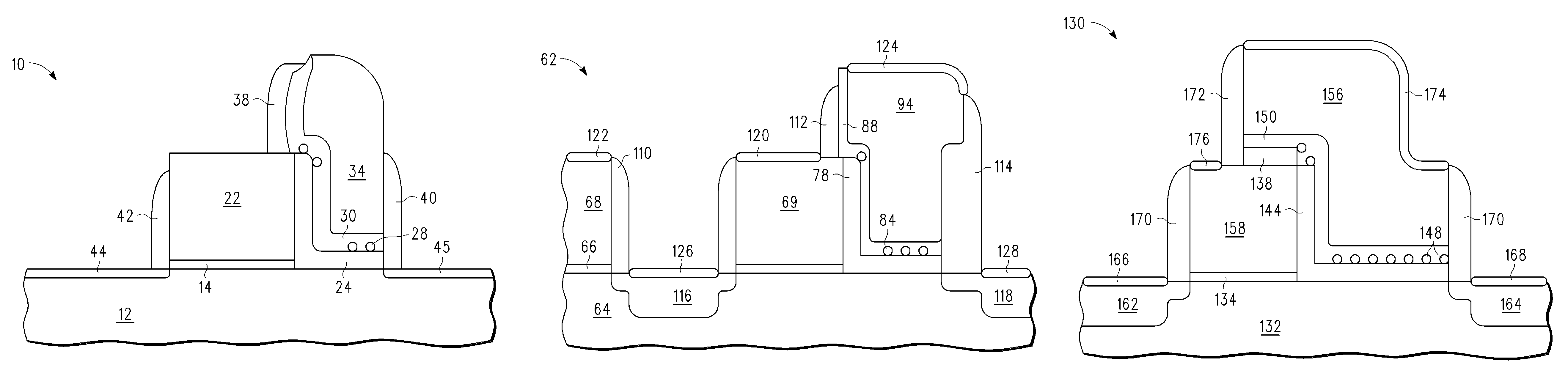
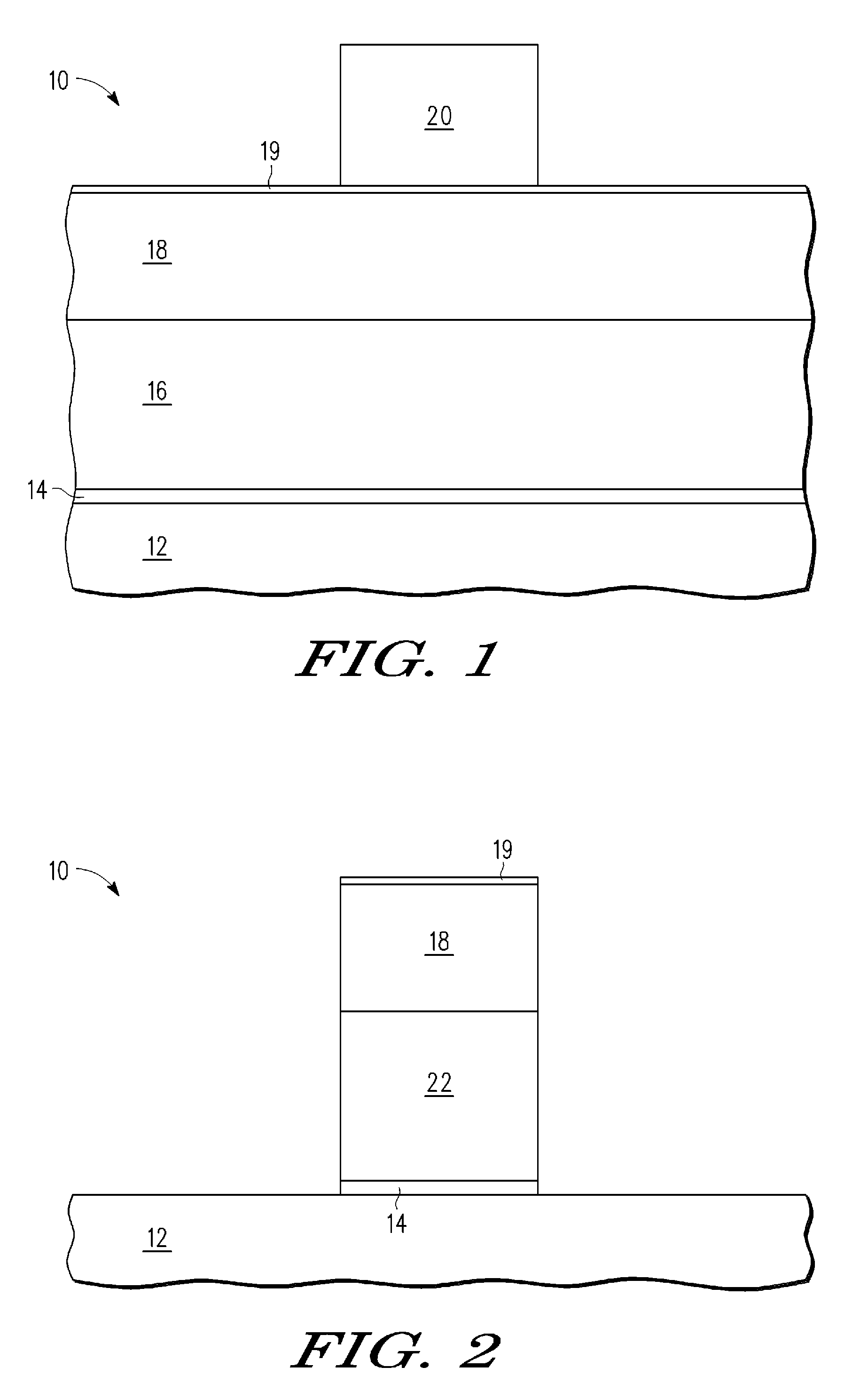
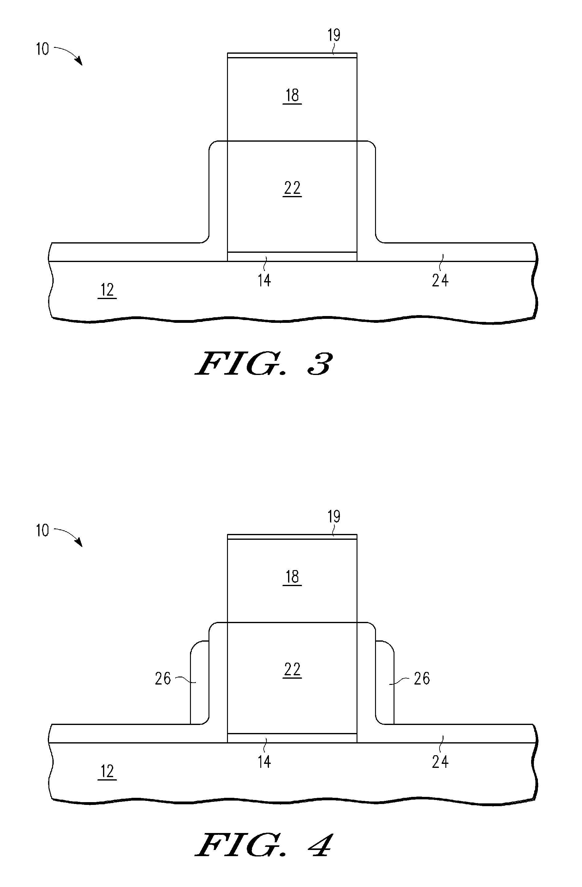
[0009]Illustrated in FIG. 1 is a cross-sectional view of a semiconductor memory device 10. A semiconductor substrate 12 is provided. The semiconductor substrate 12 described herein can be any semiconductor material or combinations of materials, such as gallium arsenide, silicon germanium, silicon-on-insulator (SOI), silicon, monocrystalline silicon, the like, and combinations of the above. Overlying the semiconductor substrate 12 is a dielectric layer 14 that functions as an insulating layer. In one form the dielectric layer 14 is an oxide and is thermally grown. In another form the oxide may be deposited on the semiconductor substrate 12. In other forms the dielectric layer 14 may be a high-K material or other conventional oxide materials. Overlying the dielectric layer 14 is a layer of select gate material 16. In one form the select gate material 16 is a polysilicon layer. In another form the select gate material 16 may be formed of any of various metals or metal alloys. Overlying...


PUM


Abstract

A method forms a split gate memory device. A layer of select gate material over a substrate is patterned to form a first sidewall. A sacrificial spacer is formed adjacent to the first sidewall. Nanoclusters are formed over the substrate including on the sacrificial spacer. The sacrificial spacer is removed after the forming the layer of nanoclusters, wherein nanoclusters formed on the sacrificial spacer are removed and other nanoclusters remain. A layer of control gate material is formed over the substrate after the sacrificial spacer is removed. A control gate of a split gate memory device is formed from the layer of control gate material, wherein the control gate is located over remaining nanoclusters.

Description

BACKGROUND[0001]1. Field[0002]This disclosure relates generally to semiconductors, and more specifically, to semiconductor memories and the manufacture thereof.[0003]2. Related Art[0004]Split gate memory cells have found a particular use in non-volatile memories (NVMs) that have many applications. A split gate memory cell has two distinguishable channel regions, respectively controlled by a select gate and a control gate, which are electrically separated by a dielectric. The select gate channel acts as an access device to select the memory cell under the control gate during read or program operations. A particular concern in any memory device is to have a sufficient voltage differential between program and erase states. This voltage differential may be considered as a memory window for differentiating between program and erase modes. Efficient removal of electrons from the storage element(s) during an erase operation helps to increase the size of the memory window and therefore impr...

Claims


Application Information

Patent Timeline
Patent Type & Authority Patents(United States)
IPC IPC(8): H01L21/336
CPCB82Y10/00H01L27/11521H01L27/115H01L21/28273H01L29/40114H10B69/00H10B41/30
Inventor MURALIDHAR, RAMACHANDRANRAO, RAJESH A.HERRICK, MATTHEW T.RAMANI, NARAYANAN C.STEIMLE, ROBERT F.
Owner NORTH STAR INNOVATIONS
Why Eureka
Try Eureka