Thin film transistor liquid crystal display and manufacturing method thereof

a technology of thin film transistor and liquid crystal display, which is applied in the direction of transistors, optics, instruments, etc., can solve the problems of reducing the quality of tft-lcd and harming the properties of tft, and achieve the effect of improving tft quality

Inactive Publication Date: 2008-09-09
AU OPTRONICS CORP
View PDF8 Cites 6 Cited by
  • Summary
  • Abstract
  • Description
  • Claims
  • Application Information

AI Technical Summary

Benefits of technology

[0007]An object of the present invention is to provide a method for forming a thin film transistor liquid crystal display (TFT-LCD) using metallic electrodes as a mask to remove the unwanted amorphous silicon layer when forming the source / drain electrodes. This method avoids the problems resulting from unwanted amorphous silicon layer, and enhances the TFT quality.
[0008]Another object of the present invention is to provide a manufacturing method for forming a thin film transistor liquid crystal display (TFT-LCD) to efficiently reduce the thickness of the insulating layer by controlling the etching condition for forming the drain / source electrodes without affecting the quality of the TFT. It also increases the capacitance Cs of the storage capacitor by reducing the thickness of the insulating layer.
[0009]Yet another object of the present invention is to provide a method for forming a thin film transistor liquid crystal display (TFT-LCD) to define a shielding metal layer above a lower electrode of a storage capacitor. After the drain / source electrodes are patterned, a number of layers are formed between the lower electrode and the shielding metal layer for increasing the storage capacitor.

Problems solved by technology

During the above etching process, if any amorphous silicon is left above the insulating layer 3 at the position outside the TFT, it will harm the properties of the TFT and reduce the quality of the TFT-LCD.

Method used


Image

  • Thin film transistor liquid crystal display and manufacturing method thereof
  • Thin film transistor liquid crystal display and manufacturing method thereof
  • Thin film transistor liquid crystal display and manufacturing method thereof

Examples


first embodiment

The First Embodiment

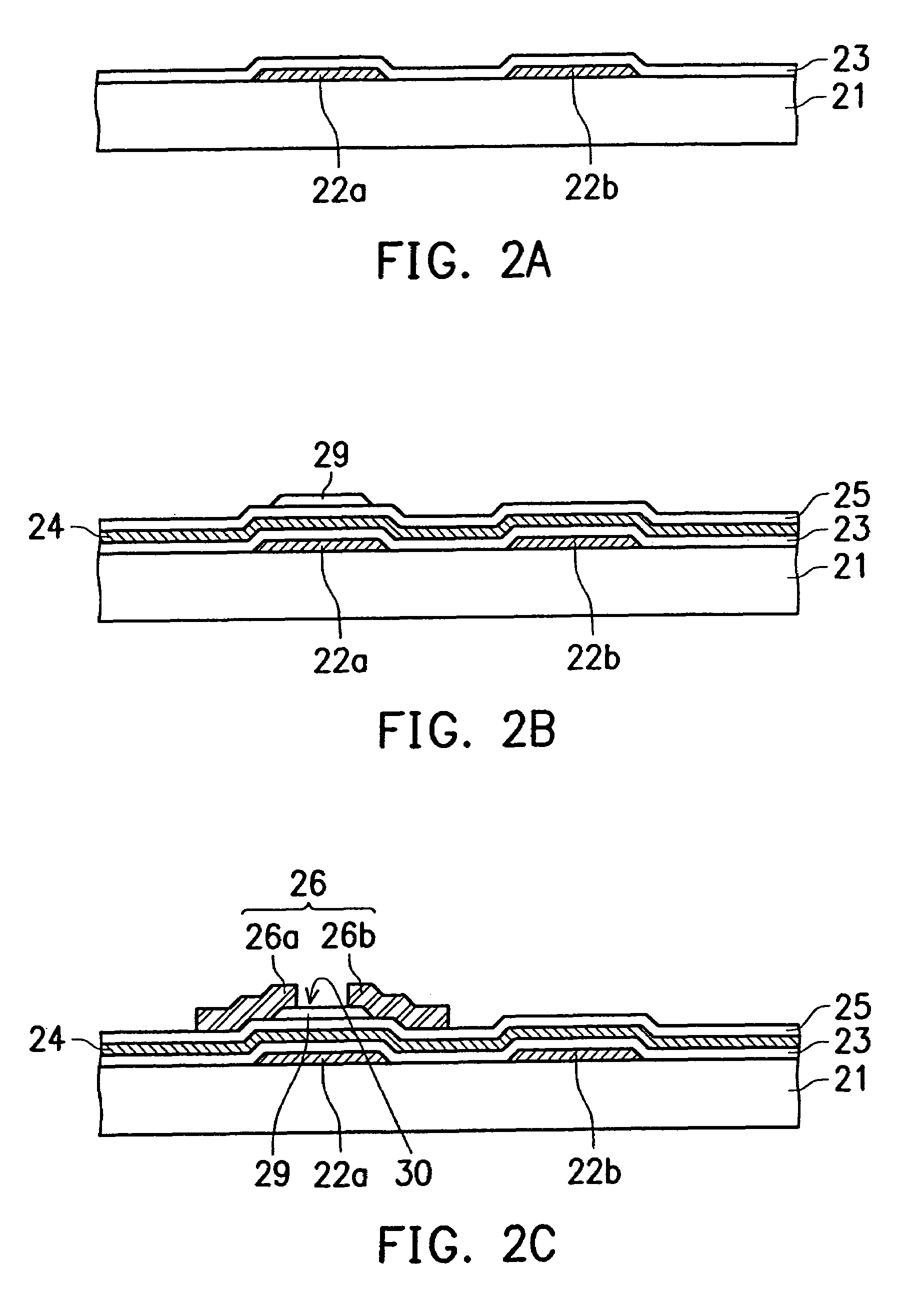
[0025]FIG. 2A to FIG. 2F are the sectional diagrams of the manufacturing process described in the first embodiment of the present invention.

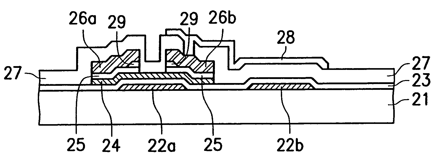
[0026]First of all, a first conductive layer 22a and a second conductive layer 22b are deposited on a substrate 21 to form a gate electrode 22a of a thin film transistor (TFT) and a bottom electrode 22b of a storage capacitor. Usually, the first and the second conductive layers 22a and 22b are metal layers, and the substrate 21 is made of glass or quartz.

[0027]Next, forming an insulating layer 23 above the first and the second conductive layers 22a, 22b and the substrate 21, as shown in FIG. 2A. Then, a semiconductor layer 24 and a doped silicon layer 25 are formed on the insulating layer 23. In the present embodiment, the semiconductor layer 24 is an amorphous silicon layer, and the doped silicon layer 25 is an n type doped poly-silicon layer.

[0028]A sacrifice layer 29 with an island shape is formed on the doped silicon laye...

second embodiment

The Second Embodiment

[0034]FIG. 3A to FIG. 3F are the sectional diagrams of the manufacturing process described in the second embodiment of the present invention. The same structures are label by the same symbolic numberings as FIG. 2A to FIG. 2F.

[0035]The process of the second embodiment is similar to that of the first embodiment. The major difference is that a shielding metal layer 31 is formed directly above the lower electrode 22b of the storage capacitor during the process for defining the source and drain electrodes 26a and 26b, as shown in FIG. 3C. Thereby, the shielding metal layer 31, the doped silicon layer 25, and the semiconductor layer 24 form a stack layer SL above the insulating layer 23 and the lower electrode 22b, as shown in FIG. 3D.

[0036]A channel 32 is defined between the source and the drain electrodes 26a and 26b. A portion of the substrate uncovered by the source electrode 26a, the drain electrode 26b, the channel 32, and the storage capacitor is defined as a ...

third embodiment

The Third Embodiment

[0038]FIG. 4A to FIG. 4F are the sectional diagrams of the manufacturing process in the third embodiment of the present invention.

[0039]First of all, a first conductive layer 42a and a second conductive layer 42b are deposited on a substrate 41 to form a gate electrode 42a of a thin film transistor (TFT) and a bottom electrode 42b of a storage capacitor.

[0040]Next, forming an insulating layer 43 above the first and the second conductive layers 42a, 42b and the substrate 41, as shown in FIG. 4A. Then, a semiconductor layer 44 is formed on the insulating layer 43. In the present embodiment, the semiconductor layer 44 is an amorphous silicon layer.

[0041]A sacrifice layer 49 with an island shape is then formed on the semiconductor layer 44, and directly above the first conductive layer 42a. Next, a doped silicon layer 45 is formed on the island-shaped sacrifice layer 49 and the semiconductor layer 44. The doped silicon layer 45 can be an n type doped poly-silicon lay...


PUM

PropertyMeasurementUnit
transparent conductiveaaaaaaaaaa
period of timeaaaaaaaaaa
timeaaaaaaaaaa

Abstract

A manufacturing method and the structure of a thin film transistor liquid crystal display (TFT-LCD) are disclosed. The TFT-LCD uses metal electrodes as a mask to thoroughly remove the unwanted semiconductor layer during the etching process for forming the source and drain electrodes. This manufacturing method can reduce the problems caused by the unwanted semiconductor layer, hence improving the quality of the TFT.

Description

CROSS-REFERENCE TO RELATED APPLICATIONS[0001]This patent application is a divisional application of U.S. Ser. No. 09 / 884,286, filed on Jun. 19, 2001 now U.S. Pat. No. 6,649,933, which claims priority to Taiwanese Application No. 89112829, filed on Jun. 29, 2000.BACKGROUND OF THE INVENTION[0002]1. Field of the Invention[0003]The present invention relates to a thin film transistor and the manufacturing method thereof, and more particularly to a thin film transistor used in a thin film transistor liquid crystal display.[0004]2. Description of the Related Art[0005]In an active matrix liquid crystal displays, a thin film transistor (TFT) is commonly adopted for good driving and switching capabilities. FIG. 1 shows the essential components of a TFT used in a thin film transistor liquid crystal display (TFT-LCD). The substrate 1 is made from glass or quartz. A metal layer 2a is used as the gate electrode of the TFT. The electrode 2b is an electrode of a storage capacitor. A insulating laye...

Claims


Application Information

Patent Timeline
Patent Type & Authority Patents(United States)
IPC IPC(8): H01L31/0376G02F1/1362G02F1/1368H01L21/336H01L21/77H01L21/84H01L27/12H01L27/13H01L29/417H01L29/786
CPCH01L29/41733H01L29/66765H01L29/78618H01L27/1288G02F1/1368H01L27/1255H01L27/124G02F1/136213
Inventor WONG, JIA-FAM
Owner AU OPTRONICS CORP
Why Eureka
Try Eureka