Device and method for inspecting photomasks and products fabricated using the same

a technology of photomasks and products, applied in the direction of semiconductor/solid-state device testing/measurement, image enhancement, instruments, etc., can solve the problem of generating false defects and mistakingly, and achieve the effect of reducing the time from inspection to repair

Inactive Publication Date: 2008-09-09
FUJITSU MICROELECTRONICS LTD
View PDF7 Cites 37 Cited by
  • Summary
  • Abstract
  • Description
  • Claims
  • Application Information

AI Technical Summary

Benefits of technology

[0009]In view of the foregoing, it is an object of the present invention to provide an inspection device capable of reducing the time from inspection to repair.

Problems solved by technology

However, the conventional inspection device 100 has a problem in that when sensitivity is raised, it mistakenly generates a false defect even if that location is not a defect.

Method used


Image

  • Device and method for inspecting photomasks and products fabricated using the same
  • Device and method for inspecting photomasks and products fabricated using the same
  • Device and method for inspecting photomasks and products fabricated using the same

Examples


Embodiment Construction

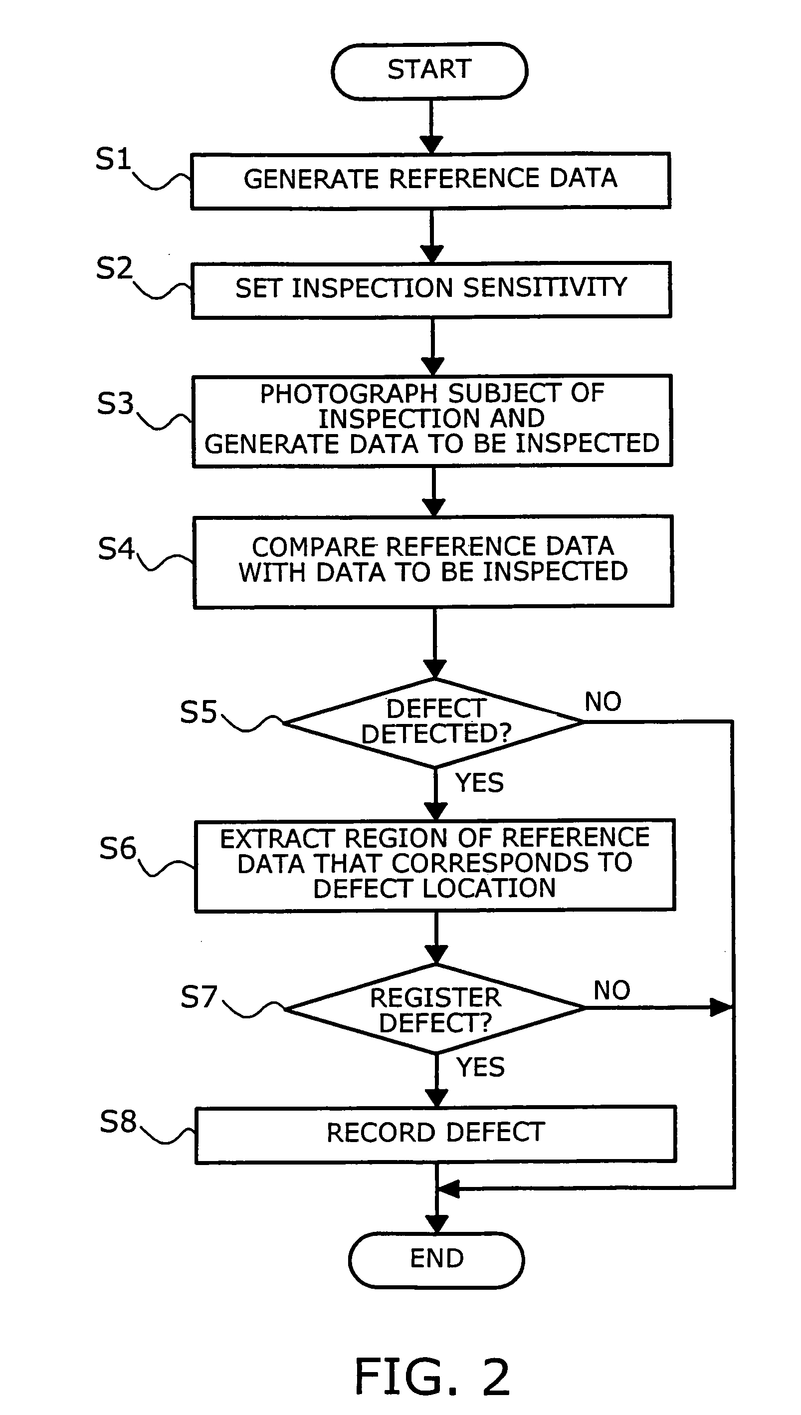
[0026]Preferred embodiments of the present invention will be described below with reference to the accompanying drawings.

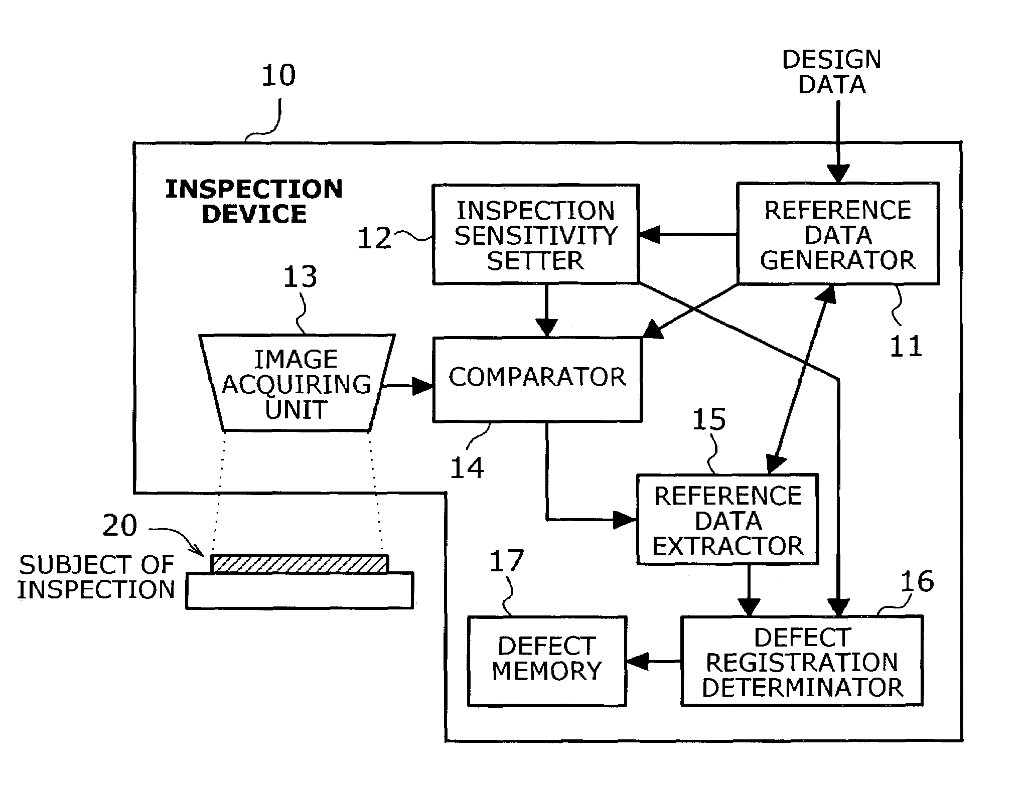
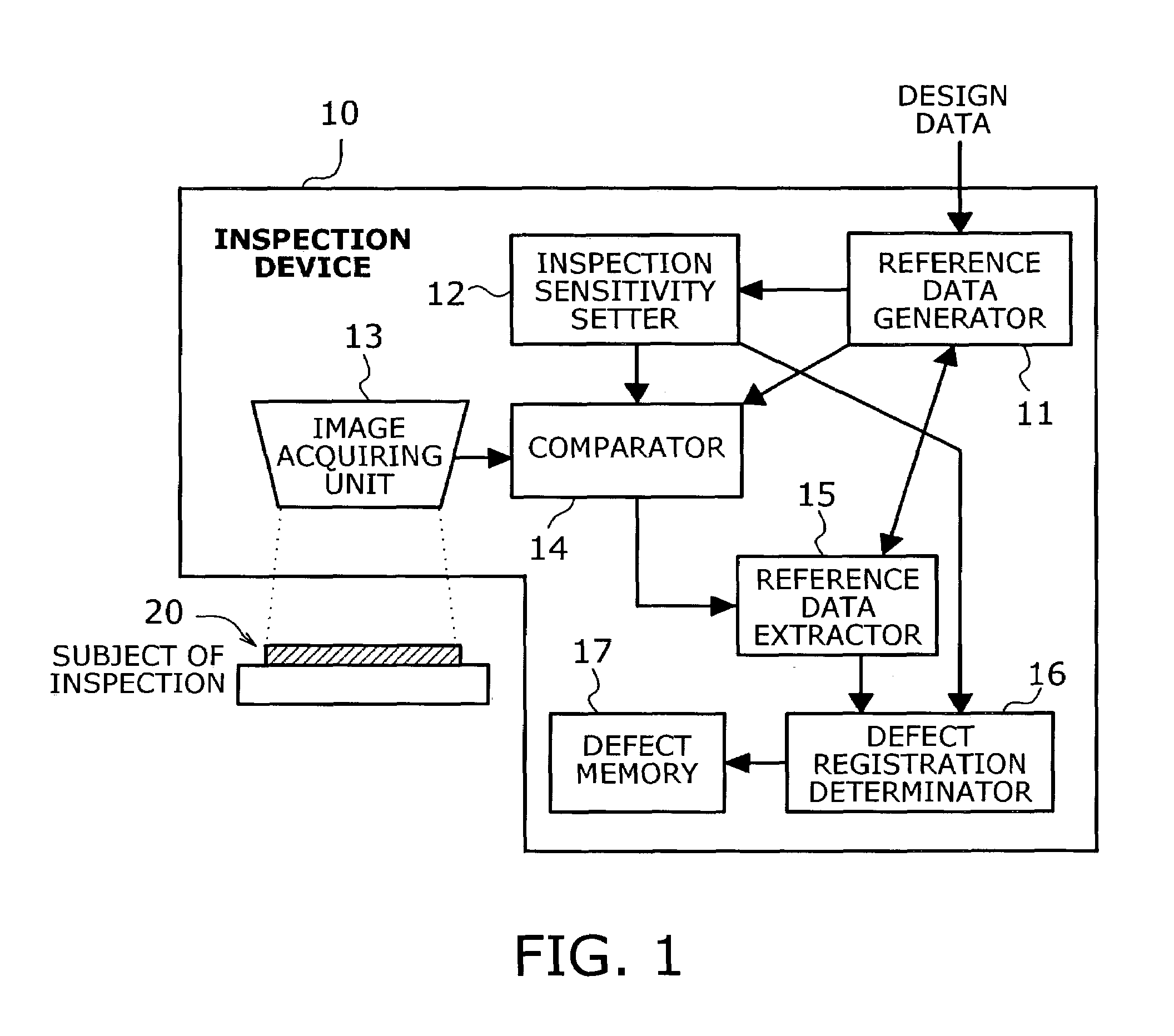
[0027]FIG. 1 is a block diagram that shows the concept of an inspection device according to the invention. This inspection device 10 identifies defects on the subject of inspection including photomasks or products fabricated using photomasks. Photomasks include reticles used with lithography equipment (known as steppers) for producing semiconductor chips and other microelectronic devices. The products that can be tested with the proposed inspection device 10 include wafers, substrates, circuit boards, and other devices on which patterns are formed. All those things can be the subject of the inspection according to the present invention, although in actual implementations inspection devices may be designed for a particular type of photomasks or products.

[0028]According to the present invention, the inspection device 10 is made up of: (a) a reference data generator ...


PUM

PropertyMeasurementUnit
sizeaaaaaaaaaa
lengthaaaaaaaaaa
sizeaaaaaaaaaa

Abstract

An inspection device for photomasks and products fabricated using the same, capable of reducing the time from inspection to repair. A reference data generator generates reference data that is based on design data and includes sensitivity class codes that differentiate designated pattern functions such as signal lines and power supply lines by means of inspection sensitivity. Then an inspection sensitivity setter allocates the desired inspection sensitivity for each sensitivity class code. An image acquiring unit photographs a subject of inspection (e.g., photomask or wafer), and a comparator detects a defect by comparing the photographed image with the reference data. When a defect is found, a reference data extractor extracts the region of the reference data that corresponds to the defect location. A defect registration determinator refers to the sensitivity class codes for the region and determines whether to register the defect. This reduces the number of defects that are registered.

Description

CROSS-REFERENCE TO RELATED APPLICATIONS[0001]This application is based upon and claims the benefits of priority from the prior Japanese Patent Application No. 2002-199595, filed on Jul. 9, 2002, the entire contents of which are incorporated herein by reference.BACKGROUND OF THE INVENTION[0002]1. Field of the Invention[0003]The present invention relates to an inspection device and method, and particularly to a device and method for inspecting photomasks and products fabricated using the same.[0004]2. Description of the Related Art[0005]As part of the advancing miniaturization of large-scale integrated circuits (LSI), recently the degree of precision is increasing not only for patterned wafers, but also for the photomasks such as reticles that are used when manufacturing LSI chips. This leads to a demand for a more sensitive inspection device that can detect smaller defects on a photomask or fabricated wafer.[0006]FIG. 12 is a block diagram that shows a conventional inspection device....

Claims


Application Information

Patent Timeline
Patent Type & Authority Patents(United States)
IPC IPC(8): G06K9/00G06F9/45G01N21/956G03F1/84G06T7/00H01L21/027H01L21/66
CPCG01N21/95607G06T7/0006G03F1/84G06T2207/30148
Inventor HORIE, TSUTOMUOHTA, KAZUTOSHI
Owner FUJITSU MICROELECTRONICS LTD
Why Eureka
Try Eureka