Small thin film movable element, small thin film movable element array and method of driving small thin film movable element array
- Summary
- Abstract
- Description
- Claims
- Application Information
AI Technical Summary
Benefits of technology
Problems solved by technology
Method used
Image
Examples
first embodiment
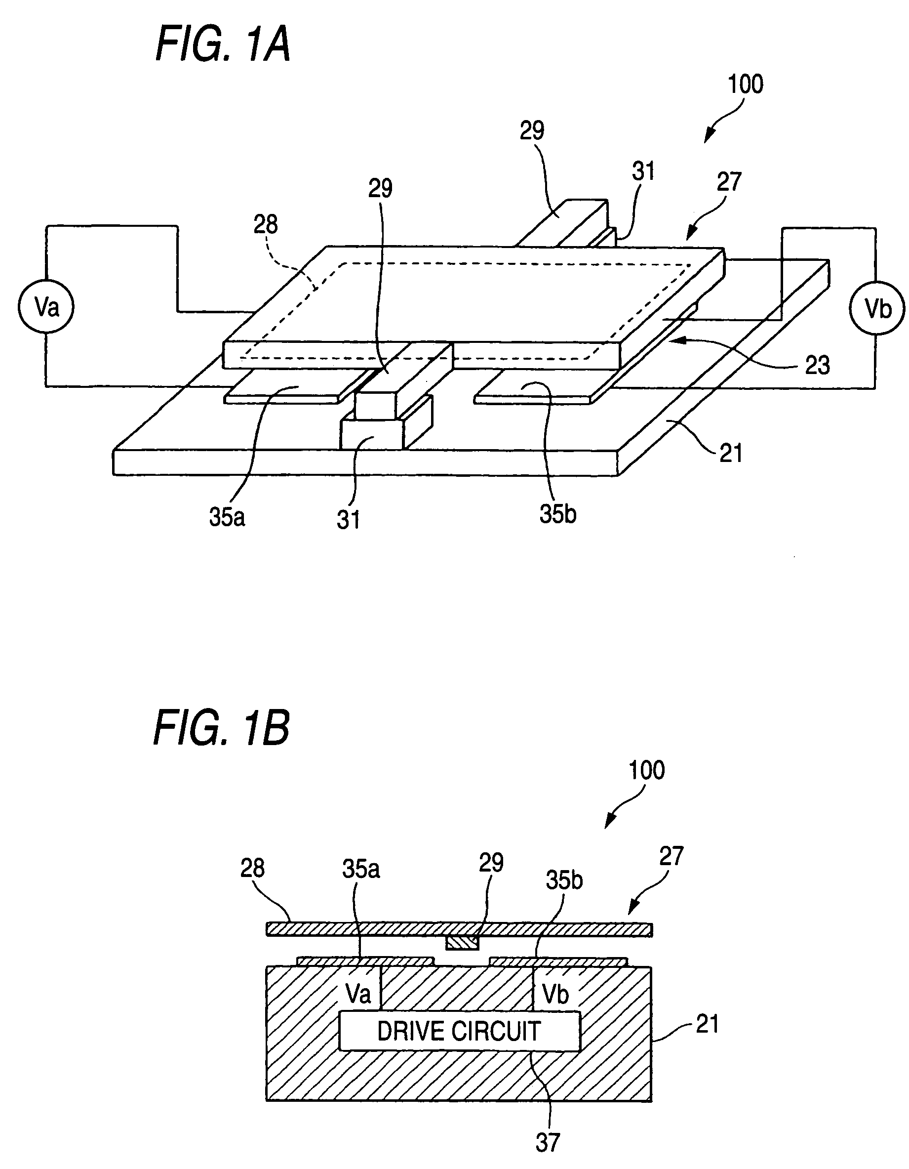
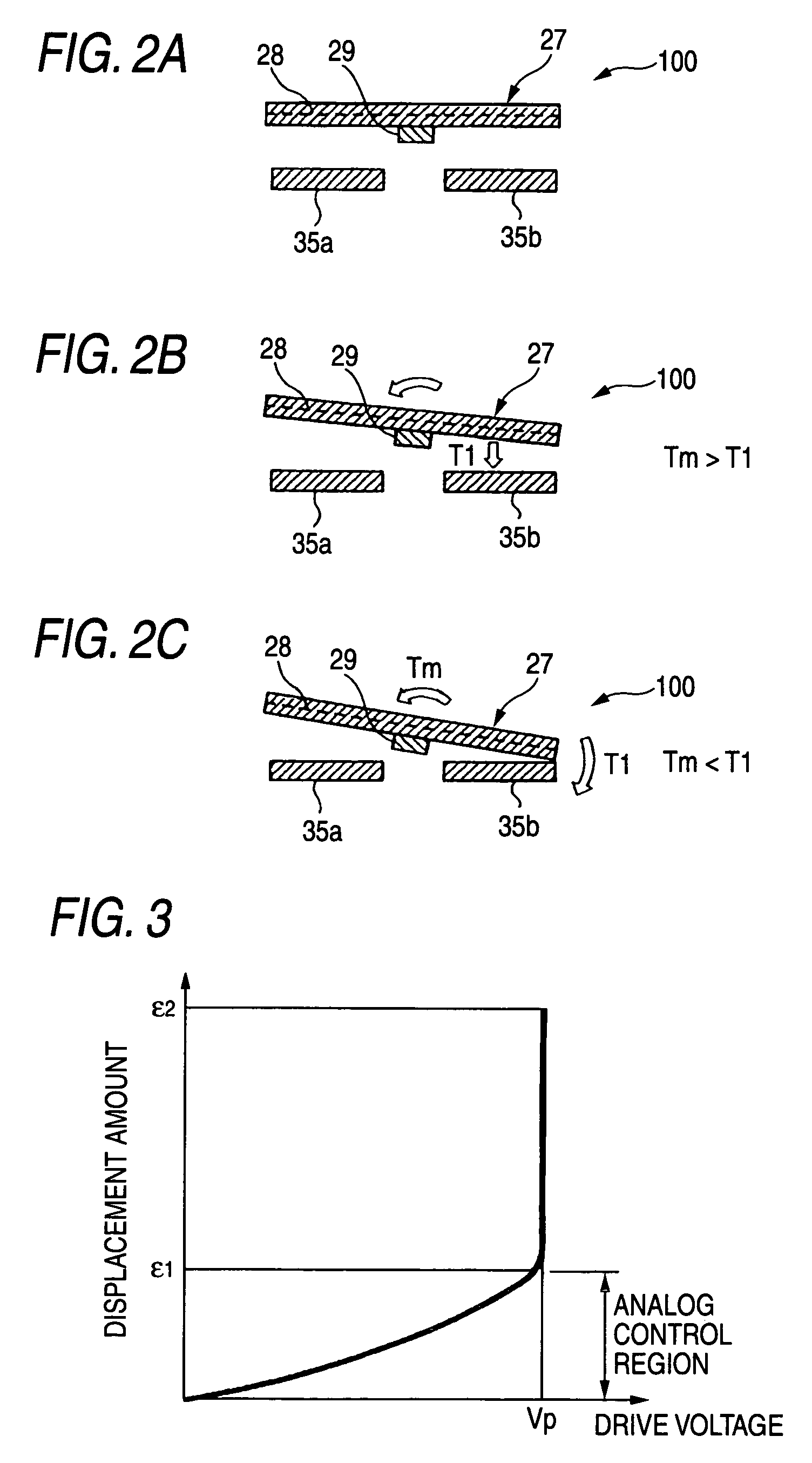
[0067]FIGS. 1A and 1B illustrate conceptual views showing a small thin film movable element according to the invention, FIGS. 2A to 2C illustrate explanatory views of operation showing an operational procedure in applying a static pull-in voltage of the small thin film movable element shown in FIG. 1, FIG. 3 is an explanatory view showing a correlation between a displacement amount and a drive voltage operated to a movable portion in applying the static pull-in voltage, and FIGS. 4A to 4C illustrate explanatory views of operation showing an operational procedure in applying a dynamic pull-in voltage of the small thin film movable element shown in FIG. 1.
[0068]A small thin film movable element 100 according to the embodiment includes a movable portion 27 in a shape of a small piece arranged in parallel with a board 21 by way of a gap 23, hinges 29, 29 constituting support portions extended from both edge portions of the movable portion 27, and spacers 31, 31 for supporting the movabl...
second embodiment
[0142]Next, a small thin film movable element according to the invention will be explained.
[0143]FIG. 20 illustrates conceptual views showing a second embodiment of a small thin film movable element according to the invention.
[0144]According to a small thin film movable element 200 according to the embodiment, one end of a movable portion 51 is supported to be fixed by the board 21 by way of the hinges 29, 29, the spacer 31, 31. That is, the movable portion 51 is constituted by a shape of a cantilever constituting a free end by other end thereof. Further, the first address electrode 35a is provided on the board 21 to be opposed to the free end of the movable portion 51, and an opposed side of the first address electrode 35a interposing the movable portion 51 is provided with the second address electrode 35b formed at an opposed board, not illustrated.
[0145]Also in the small thin film movable element 200 having such a constitution, the voltage Va, Vb applied between the first address...
third embodiment
[0146]Next, a small thin film movable element according to the invention will be explained.
[0147]FIGS. 21A and 21B illustrate conceptual views showing a third embodiment of a small thin film movable element according to the invention.
[0148]A small thin film movable element 300 according to the embodiment is an element of a so-to-speak parallel flat plate type, and both ends of a movable portion 61 in a flat plate shape having a conductivity and a flexibility are fixed to an insulating film 63 formed on the board 21 by way of the predetermined gap 23. A lower side of the movable portion 61 of the board 21 is arranged with the first address electrode 35a by way of the insulating film 63, further, an upper side of the movable portion 61 is arranged with the second address electrode 35b by way of an insulating film 65. That is, the movable portion 61 is constituted by a shape of a both support beam both ends of which are supported between the first address electrode 35a and the second a...
PUM
 Abstract
Description
Claims
Application Information


