Integrated circuit communication techniques

a communication technique and integrated circuit technology, applied in the field of integrated circuit devices, can solve the problems of long delay of these long lines, severe degradation of their transition time and propagation delay, and not bandwidth, but performan

Active Publication Date: 2008-10-21
TAHOE RES LTD
View PDF16 Cites 209 Cited by
  • Summary
  • Abstract
  • Description
  • Claims
  • Application Information

AI Technical Summary

Benefits of technology

[0019]There is thus provided in accordance with a preferred embodiment of the present invention a semiconductor device comprising a multiplicity of logic blocks, and connections between said blocks where at least one of the connections includes, a differential driver, two wires adjacent to each other, and at least one clocked current sensing receiver, which are connected so as to transmit and receive differential current pulses for the purposes of transferring data between the logic blocks, and clocked to reduce power.
[0020]Furthermore, the current sensing receiver includes, differential inputs, a clock input, a latch, and a differential receiver, where the differential receiver is disabled by a signal from a clock input, to reduce the power consumed by the receiver when not receiving data, and the transmitter may transmit multiple bits of data on the two wires prior to the current sensing receiver receiving the first bit of data.
[0022]There is also provided, in accordance with another preferred embodiment of the present invention, a semiconductor device including a first logic block, a second logic block, and a high speed connection for transferring logic information from the first to the second logic block, where the logic information is represented by the direction of current. The second logic block includes a receiver to convert the direction of current to a normal voltage level logic representation and is powered for a small period of time to save power.
[0027]There is also provided, in accordance with yet another preferred embodiment of the present invention, an automated design tool that can synthesize and place a design starting from a high level design description so that, when two logic blocks are placed far apart and a high speed connection is required from one logic block to a second logic block, then the synthesis and placement is done such that the second logic block will include a latch or a flip flop as part of the very first logic elements connected to the high speed connection

Problems solved by technology

The added capacitance and resistance of the wires in sub 100 nanometer processes has slowed this charging and discharging even as the transmitter's drive increases due to the shorter gate lengths, resulting in longer delays for these long lines.
Typically long metal interconnects on ICs have high resistive and capacitive losses, which severely degrades their transition times and propagation delays, as well as making them subject to adjacent signal inductive and capacitive coupling.
Clearly the problem is not bandwidth, but performance.
As the dimensions shrink and the number of interconnect layers grows, there is plenty of space for on-chip interconnect, but without improvements such as described in this disclosure, the performance of Integrated Circuits will not be improved by going to smaller process dimensions.

Method used


Image

  • Integrated circuit communication techniques
  • Integrated circuit communication techniques
  • Integrated circuit communication techniques

Examples


Embodiment Construction

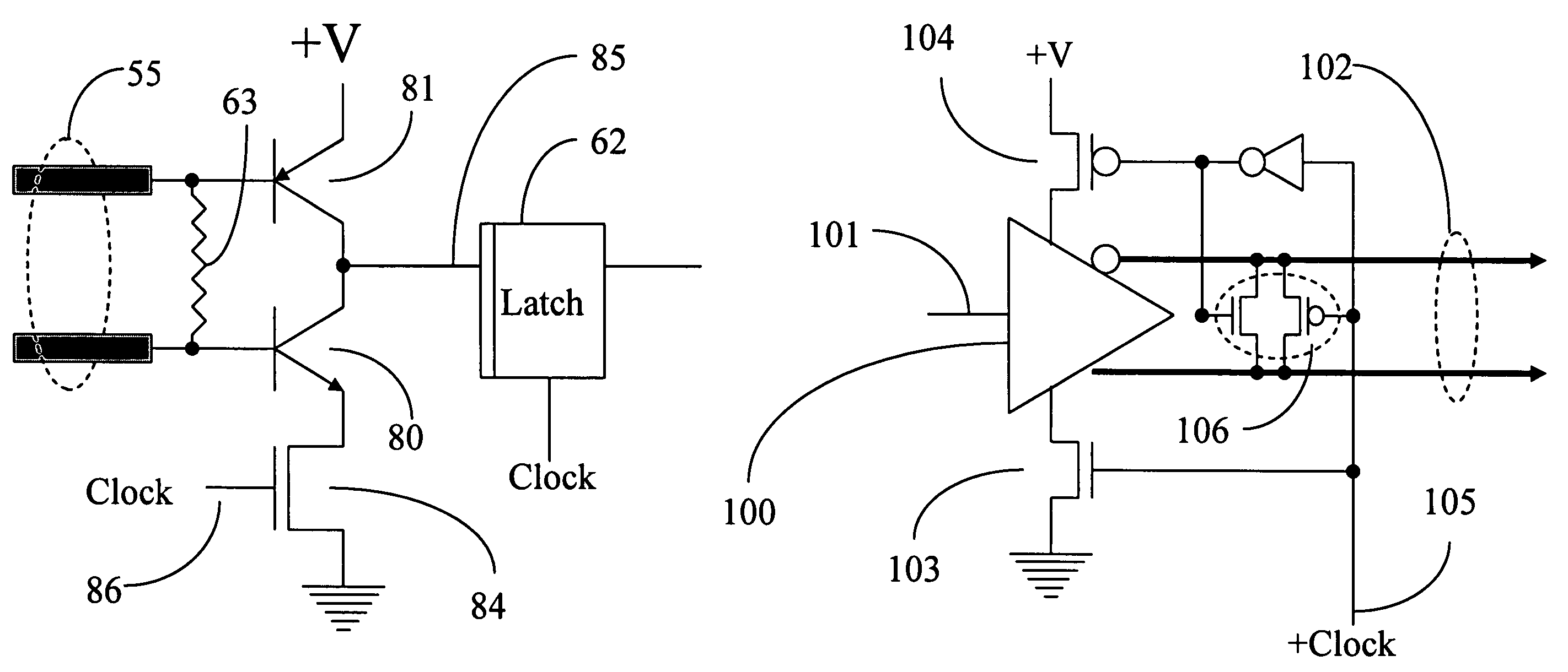
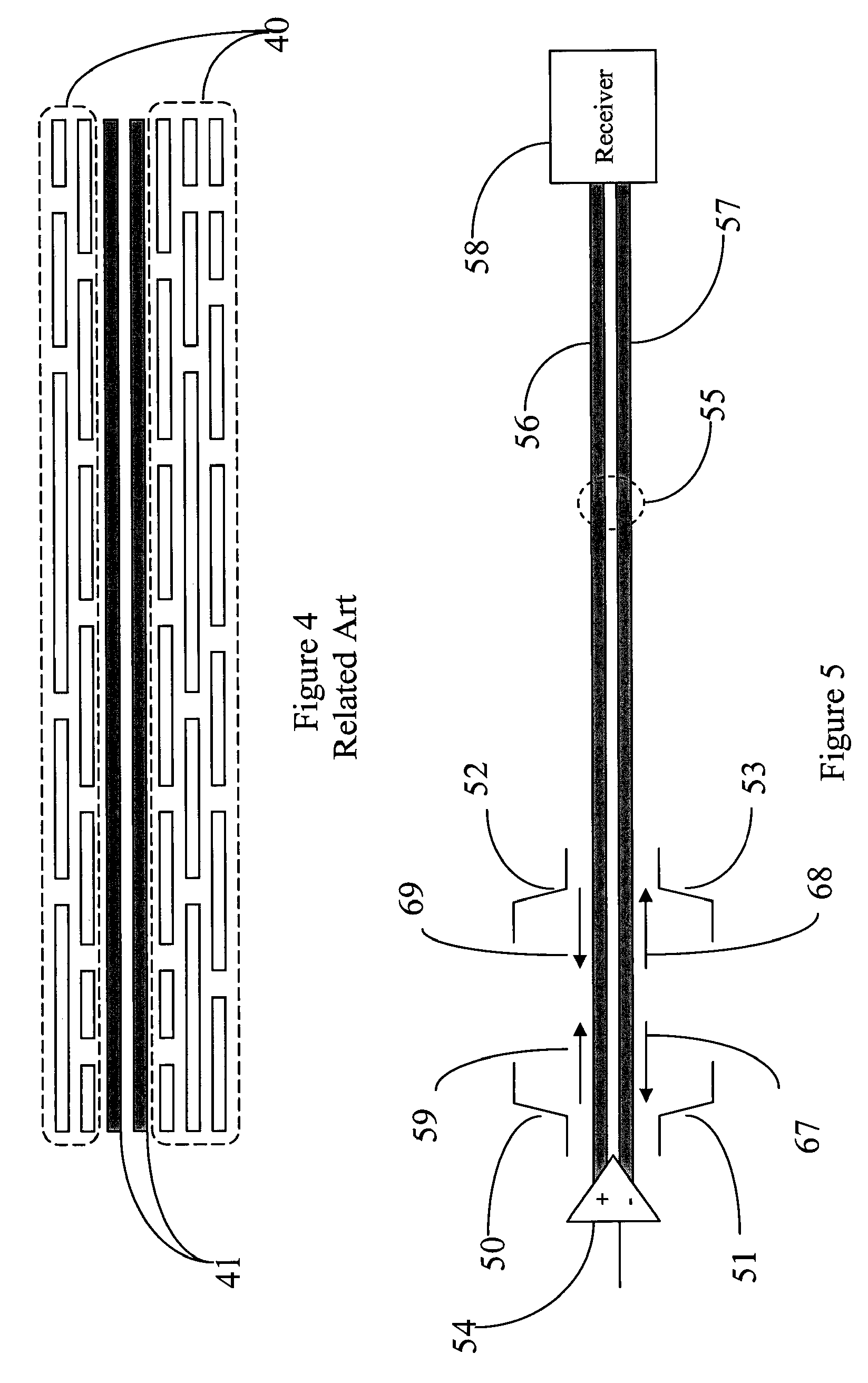
[0051]A basic concept in this disclosure is to employ differential drivers and receivers on pairs of differential transmission lines to improve the performance and bandwidth of on-chip long line communications, while keeping the power and interference from external noise to a minimum.

[0052]Reference is now made to FIG. 5. In one embodiment of the present invention, a differential voltage signal up 50, 51 or down 52,53 is generated by a differential driver 54, down a differential transmission line 55, further comprised of a positive 56, and a negative 57 wire, both going to a receiver 58. More importantly along with the voltage, the differential driver 54 generates corresponding current 59,67 going in the opposite directions for a signal up, and reversing directions 69,68 for a signal down. The differential signal up is comprised of positive current 59 on the positive line 56, and negative current 67 on the negative line 57. The differential signal down is comprised of a negative cur...


PUM


Abstract

An semiconductor device, containing logic blocks and high speed connections between the blocks, where the connections utilize current direction for logic representation rather than voltage level. Such high speed connections comprise differential transmitters which drive a pair of adjacent wires with differential current pulses that are received by a differential receiver which may be put in a low power state between transmissions.

Description

FIELD OF THE INVENTION[0001]The present invention relates to integrated circuit (IC) devices as well as to methods for transmitting and receiving signals within such integrated circuit devices.BACKGROUND OF THE INVENTION[0002]The following U.S. patents are believed to represent the current state of the art: U.S. Pat. Nos. 5,963,495, 6,703,907, 6,529,085, 6,815,980, 6,388,495, and 6,556,628 . These patents all relate to prior art with respect to the current patent.[0003]When semiconductor's smallest dimensions were much larger than a micron, line spaces and widths for the metal interconnect between the transistors were much larger than their thickness. Also there were only a few layers of metal. As a result signals propagated down wires in a fashion similar to a resistive transmission line. The primary components of delay at that time were the capacitance to the ground plane and the resistance of the wire.[0004]FIG. 1 shows a side view of such wires 10 and vias 11 between two layers ...

Claims


Application Information

Patent Timeline
Patent Type & Authority Patents(United States)
IPC IPC(8): H03K19/00
CPCH03K5/2481H03K19/0016H03K19/01812H04L25/0272
Inventor OR-BACH, ZVIAPOSTOL, ADRIANCOOKE, LAURENCE H.
Owner TAHOE RES LTD
Why Eureka
Try Eureka