Method of manufacturing semiconductor nanowires

a manufacturing method and technology of nanowires, applied in the direction of nanoinformatics, crystal growth process, polycrystalline material growth, etc., can solve the problems of complex process, large amount of laboratory equipment, and several monitoring, and achieve the effect of promoting the uniform growth of calcified minerals

Inactive Publication Date: 2008-10-28
TEXAS CHRISTIAN UNIVERSITY
View PDF24 Cites 28 Cited by
  • Summary
  • Abstract
  • Description
  • Claims
  • Application Information

AI Technical Summary

Problems solved by technology

While the above technique can be used to produce silicon nanowires of high purity, the process is complicated, requires fairly extensive laboratory equipment, and requires careful monitoring of several different parameters.

Method used


Image

  • Method of manufacturing semiconductor nanowires
  • Method of manufacturing semiconductor nanowires
  • Method of manufacturing semiconductor nanowires

Examples


Embodiment Construction

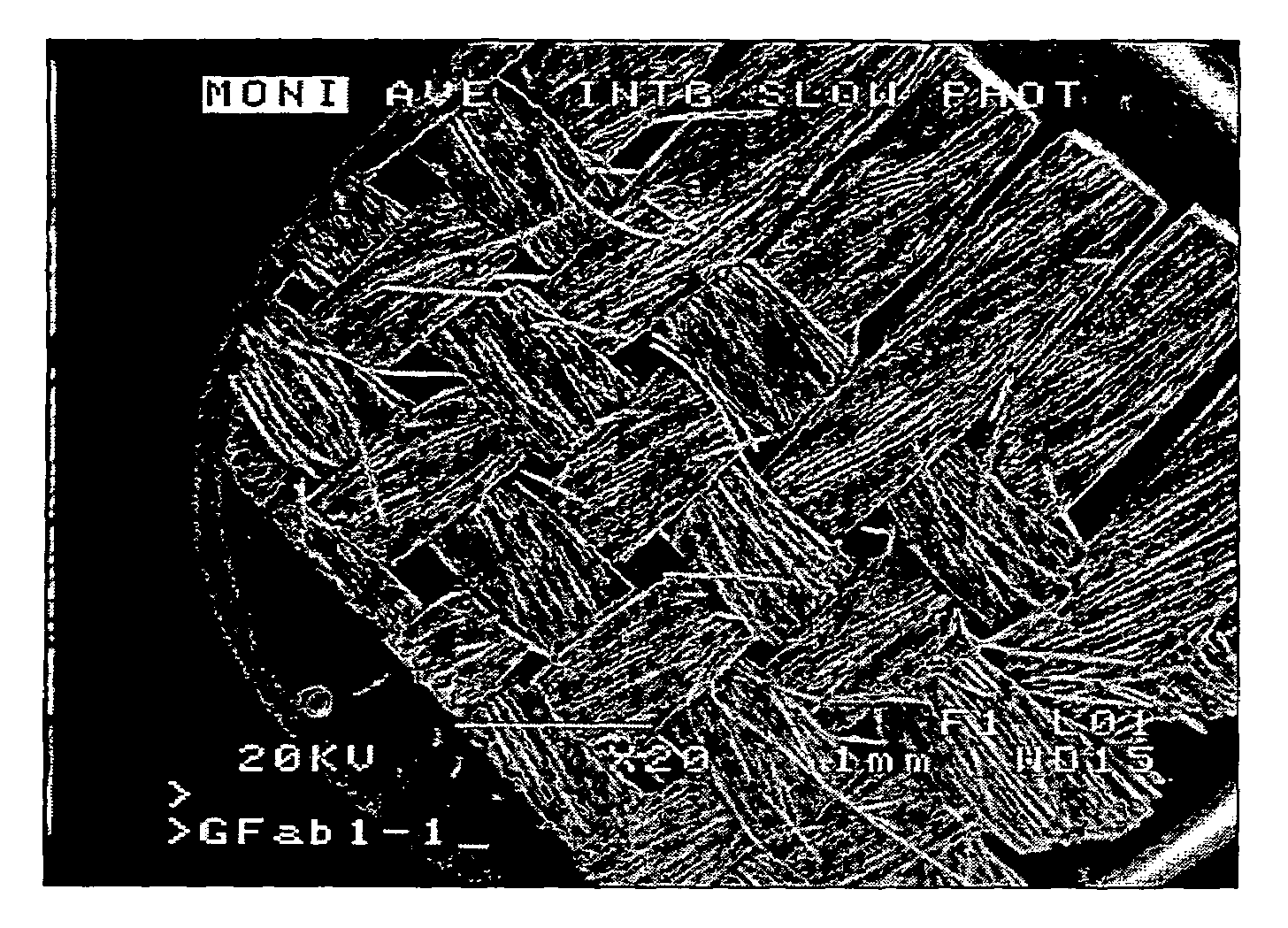
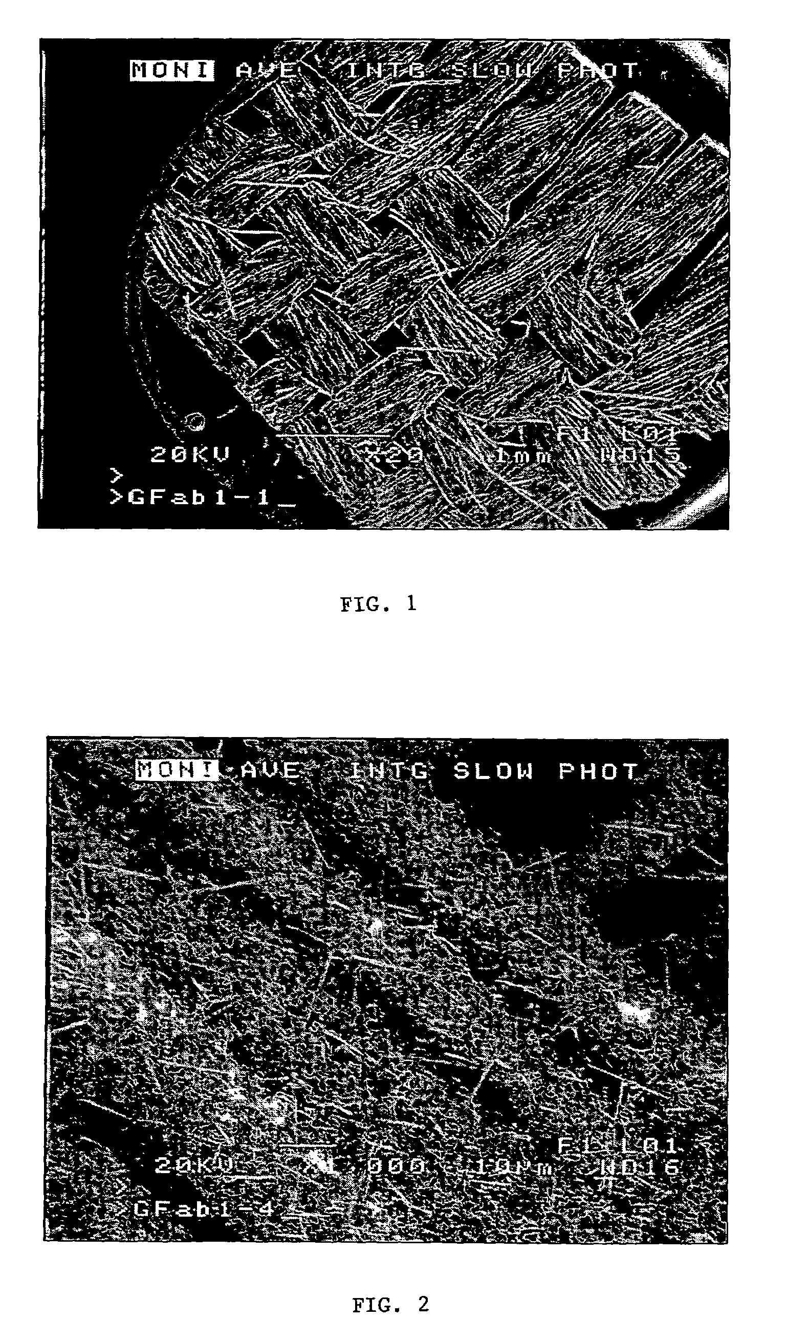
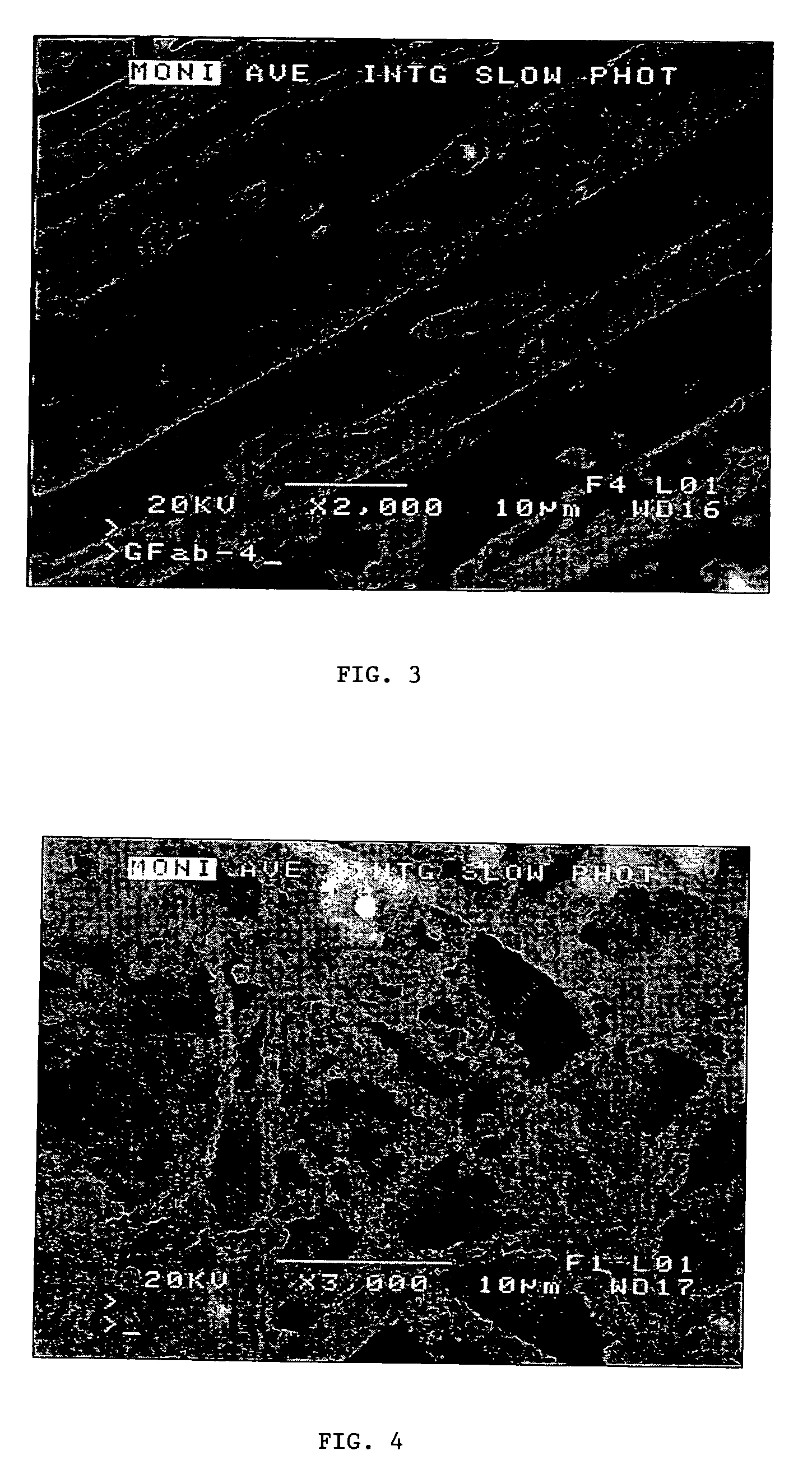
[0031]The present invention provides a relatively simple and uncomplicated method for producing semiconductor nanowires, and more specifically, silicon nanowires. For a frame of reference, the term “nanowire”, as used in the discussion which follows, generally refers to any elongated conductive or semiconductive material that includes at least one cross sectional dimension that is less than 500 nm and has an aspect ratio (length:width) of greater than 10, possibly even greater than 100. For example, in the preferred embodiment of the present invention, nanowires are grown which are on the order of 100-250 nm in width and tens of micrometers in length.

[0032]In the method of the invention, a high surface area growth of semiconductor nanowires is obtained on a conducting substrate. A selected graphite material, preferably a commercially available graphite cloth, is provided as the conducting substrate. The semiconductor nanowire is grown on the substrate and then detached from the subs...


PUM

PropertyMeasurementUnit
length:widthaaaaaaaaaa
aspect ratioaaaaaaaaaa

Abstract

A method is shown for manufacturing silicon semiconductor nanowires on graphite cloth conducting substrates. The nanowires are grown on the substrate by first depositing a thin gold film on the graphite cloth using RF sputtering. The substrate structure is then exposed to dilute silane, resulting in a uniform coating of Si nanowires on the cloth. A method is also shown for growing calcified mineral phases on such nanowire surfaces as well as for the incorporation of anti-osteoporotic drugs or anti-bacterial agents onto the surface of the nanowires. Lastly, a method is shown for promoting the growth of bone-forming cells onto the nanowire materials by exposing specially treated nanowires to bone marrow cells.

Description

BACKGROUND OF THE INVENTION[0001]1. Field of the Invention[0002]The present invention relates generally to the manufacture of semiconductor nanowires and, more specifically, to the manufacture of silicon nanowires on conducting substrates, and to selected applications and end uses of the resulting structures.[0003]2. Description of the Prior Art[0004]Nanostructures, which include but are not limited to nanofibers, nanowires and nanocrystals, have potential uses in a variety of fields including electrical, chemical and optical applications. Likewise, these unique structures appear to offer great potential advantages in the biomedical field. Researchers at Texas Christian University and others are presently developing semiconductor nanowires, specifically silicon (Si) nanowires, for applications relevant to biomaterials in general, and orthopedics in particular.[0005]Nanomaterials are currently known to be used in a variety of applications in the fields mentioned above. As an example ...

Claims


Application Information

Patent Timeline
Patent Type & Authority Patents(United States)
IPC IPC(8): H01L21/00
CPCB82Y10/00C30B11/12C30B29/06C30B29/60H01L21/02376H01L21/02491H01L21/02532H01L21/02603H01L21/02639H01L21/02664H01L29/0665H01L29/0673Y10S977/762
Inventor COFFER, JEFFERY L.
Owner TEXAS CHRISTIAN UNIVERSITY
Why Eureka
Try Eureka