Non-volatile programmable impedance nanoscale devices

a programmable impedance, nano-scale technology, applied in semiconductor devices, digital storage, instruments, etc., can solve the problems of large area on an electronic device, large amount of space consumed, and many of these techniques tend to be irreversibl

Active Publication Date: 2008-10-28
HEWLETT-PACKARD ENTERPRISE DEV LP
View PDF15 Cites 58 Cited by
  • Summary
  • Abstract
  • Description
  • Claims
  • Application Information

AI Technical Summary

Benefits of technology

[0011]Another embodiment, drawn to a method of tuning the programmable impedance device, includes applying at least one current pulse between the pair of electrodes in a second bias direction with an absolute value peak current, wherein the current pulse is sufficient to modify an impedance between the pair of electrodes by an impedance increase associated with the absolute value peak current.
[0012]While the specification concludes with claims particularly pointing out and distinctly claiming that which is regarded as the present invention, the advantages of this invention can be more readily ascertained from the following description of the invention when read in conjunction with the accompanying drawings in which:

Problems solved by technology

Unfortunately, many of these techniques tend to be irreversible.
This combination of multiple impedance devices creates added complexity and may consume large amounts of area on an electronic device.
Additionally, semiconductor device fabrication is becoming increasingly complex and difficult as attempts are made to reduce device size to the nanometer technology range.
While two discrete states may be sufficient and desirable for some memory or logic applications, this approach is limited.
Two-state devices also do not facilitate impedance matching, such as for high speed signal applications.

Method used


Image

  • Non-volatile programmable impedance nanoscale devices
  • Non-volatile programmable impedance nanoscale devices
  • Non-volatile programmable impedance nanoscale devices

Examples


Embodiment Construction

[0024]In the following description, micron-scale dimensions refer roughly to dimensions that range from one micrometer up to a few micrometers, sub-micron scale dimensions refer roughly to dimensions that range from 1 micrometer down to 0.05 micrometers, and nanometer scale dimensions refer roughly to dimensions that range from 1 nanometer up to 50 nanometers (0.05 micrometers).

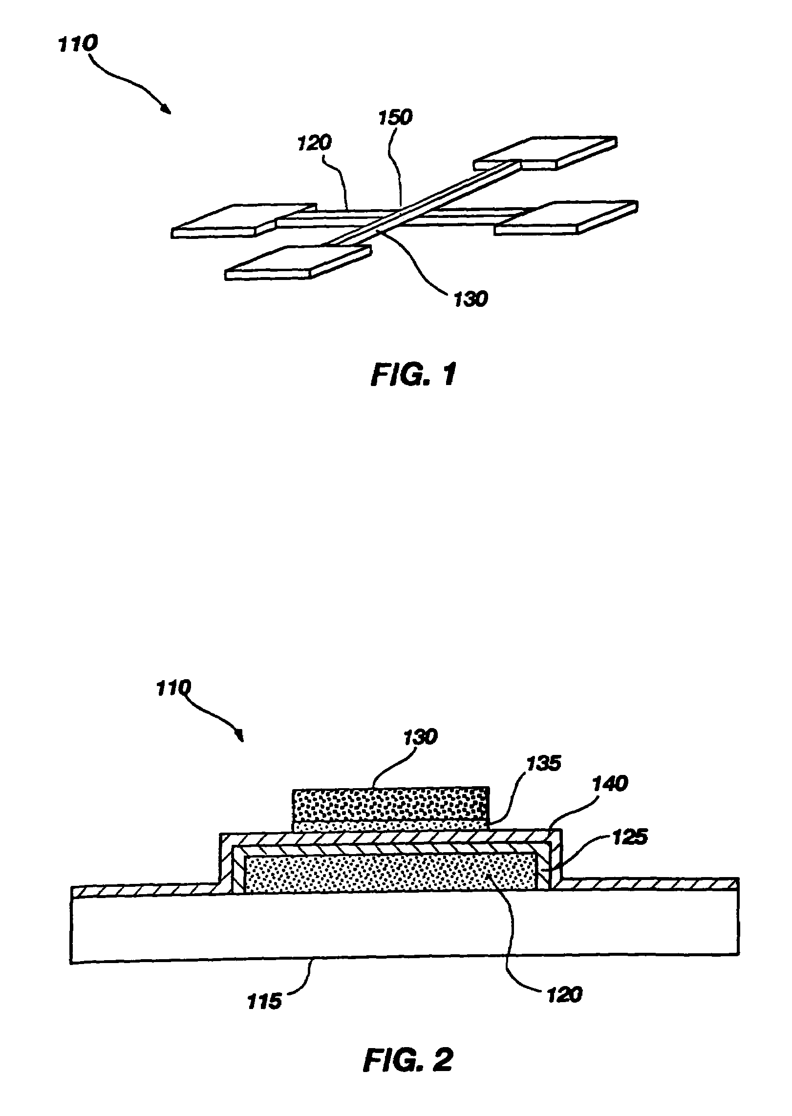
[0025]A programmable impedance device 110 according to an embodiment of the present invention, using crossed rectangular electrodes, is shown in FIGS. 1 and 2. The programmable impedance device 110 includes a first electrode 120 disposed on a substrate 115 in a first direction, a programmable material 140 disposed over at least a portion of the first electrode 120 and a second electrode 130 disposed over the programmable material 140 at a non-zero angle relative to the first electrode 120.

[0026]The programmable impedance device 110 may be formed on a variety of suitable insulating, or semiconducting substrate...


PUM


Abstract

Programmable impedance devices and methods of fabricating the devices are disclosed. The programmable impedance devices exhibit non-volatile tunable impedance properties. A programmable impedance device includes a first electrode, a second electrode and a programmable material disposed between the two electrodes. The programmable material may be disposed at a junction between the first and second electrodes.

Description

CONTRACTUAL ORIGIN OF THE INVENTION[0001]This invention was made with United States Government support under Contract No. DABT63-99-3-003 awarded by the Defense Advanced Research Projects Agency (DARPA). The United States Government has certain rights in the invention.FIELD OF THE INVENTION[0002]The present invention relates generally to nanometer-scale electronic devices (nanoelectronics), molecular electronics and more particularly to electronic devices exhibiting non-volatile programmable impedance characteristics.BACKGROUND OF THE INVENTION[0003]Electronic devices exhibiting a specific electrical impedance that may also be tuned to various impedance values while part of an electronic circuit are very useful in a variety of applications. Traditional semiconductor fabrication techniques allow fabrication of devices exhibiting a single non-volatile impedance or, in the case of a conventional transistor, a configurable, but volatile impedance. These single impedance devices may be t...

Claims


Application Information

Patent Timeline
Patent Type & Authority Patents(United States)
IPC IPC(8): G11C11/56H01L23/58
CPCB82Y10/00G11C11/5664G11C11/5685G11C13/0007G11C13/0014G11C13/0019G11C13/0069H01L27/101G11C2013/009G11C2213/32G11C2213/55G11C2213/77H01L51/0591H10K10/50
Inventor STEWART, DUNCAN R.BECK, PATRICIA A.OHLBERG, DOUGLAS A.
Owner HEWLETT-PACKARD ENTERPRISE DEV LP
Why Eureka
Try Eureka