Methods of forming a plurality of capacitors

a capacitor and electrode opening technology, applied in the field of capacitor electrode opening formation methods, can solve the problems of not being able to fabricate integrated circuitry, exceeding the depth of these peripherally formed electrodes, and not being able to uniformly form the electrode openings of the capacitor being fabricated

Inactive Publication Date: 2008-11-04
ROUND ROCK RES LLC
View PDF120 Cites 30 Cited by
  • Summary
  • Abstract
  • Description
  • Claims
  • Application Information

AI Technical Summary

Problems solved by technology

As integrated circuitry density has increased, there is a continuing challenge to maintain sufficiently high storage capacitance despite typical decreasing capacitor area.
The etch which is used to form the capacitor electrode openings can unfortunately be non-uniform across a wafer being fabricated.
For example, typically at the edge of the wafer, it is recognized that some of this area will not be usable for fabricating integrated circuitry.
Unfortunately, the etch back of the capacitor electrode-forming material to expose the outer lateral sides of the capacitor electrodes is typically wet and can exceed the depth of the these peripherally formed electrodes.
Thereby, such electrodes are no longer retained on the wafer in their original positions, and accordingly lift off the wafer and redeposit elsewhere, leading to fatal defects.

Method used


Image

  • Methods of forming a plurality of capacitors
  • Methods of forming a plurality of capacitors
  • Methods of forming a plurality of capacitors

Examples


Embodiment Construction

[0029]This disclosure of the invention is submitted in furtherance of the constitutional purposes of the U.S. Patent Laws “to promote the progress of science and useful arts” (Article 1, Section 8).

[0030]Exemplary preferred embodiments of methods of forming a plurality of capacitors are described with reference to FIGS. 1-16. U.S. Patent Application Publication No. 2005 / 0054159 A1, entitled, “Semiconductor Constructions, and Methods of Forming Capacitor Devices”, filed Dec. 10, 2003, naming H. Montgomery Manning, Thomas M. Graettinger, and Marsela Pontoh as inventors, is hereby fully incorporated by reference as if included in its entirety herein.

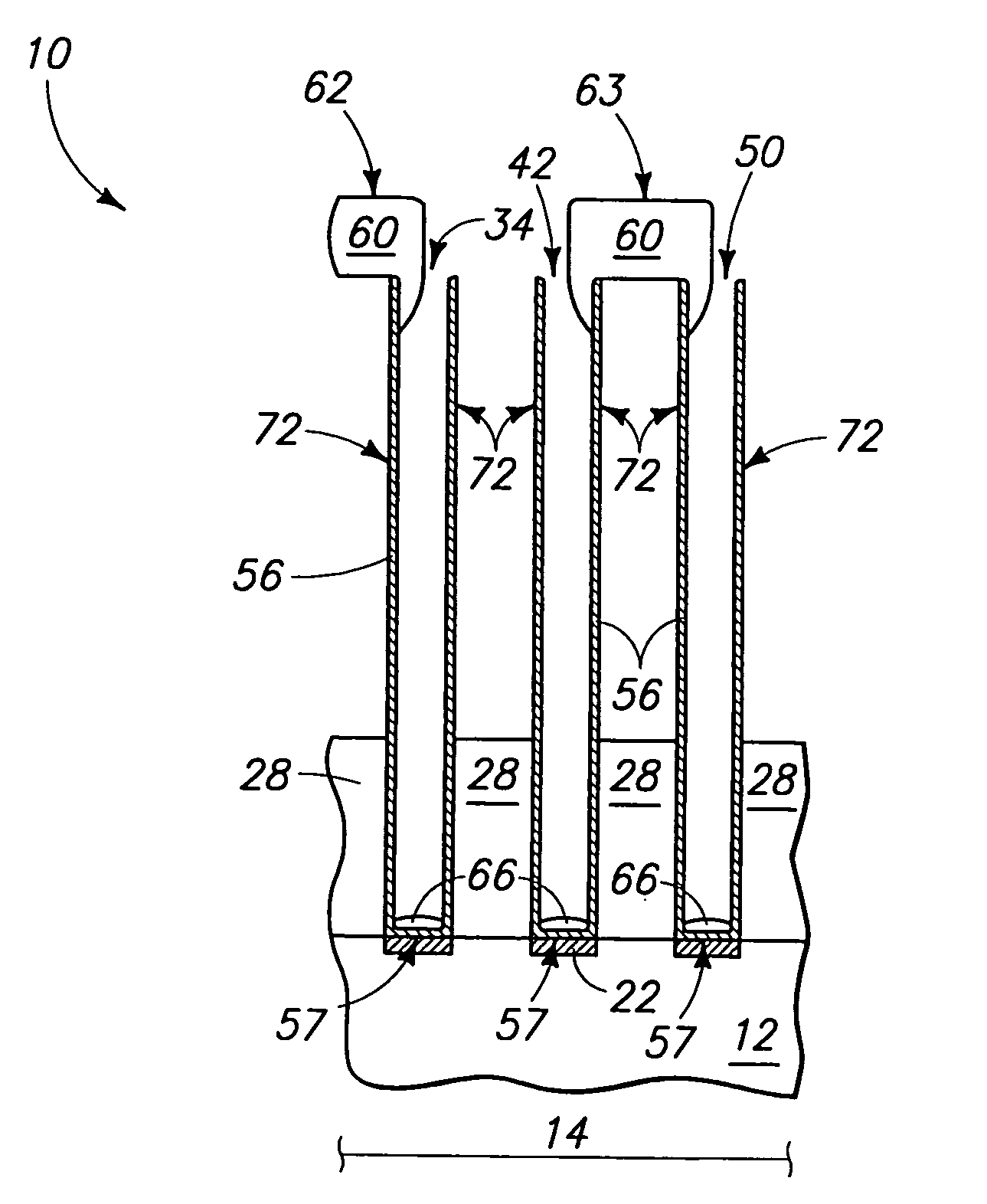
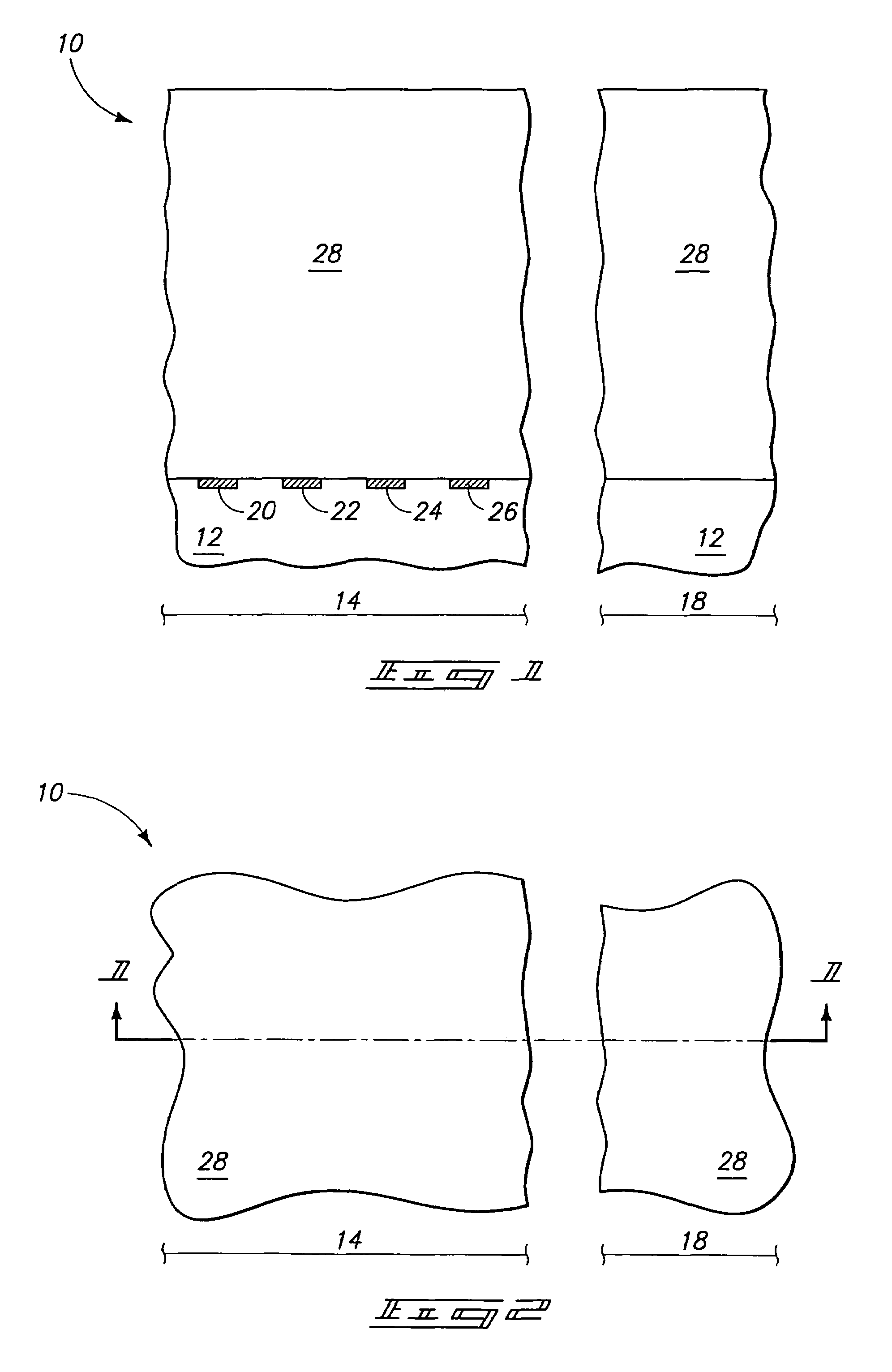
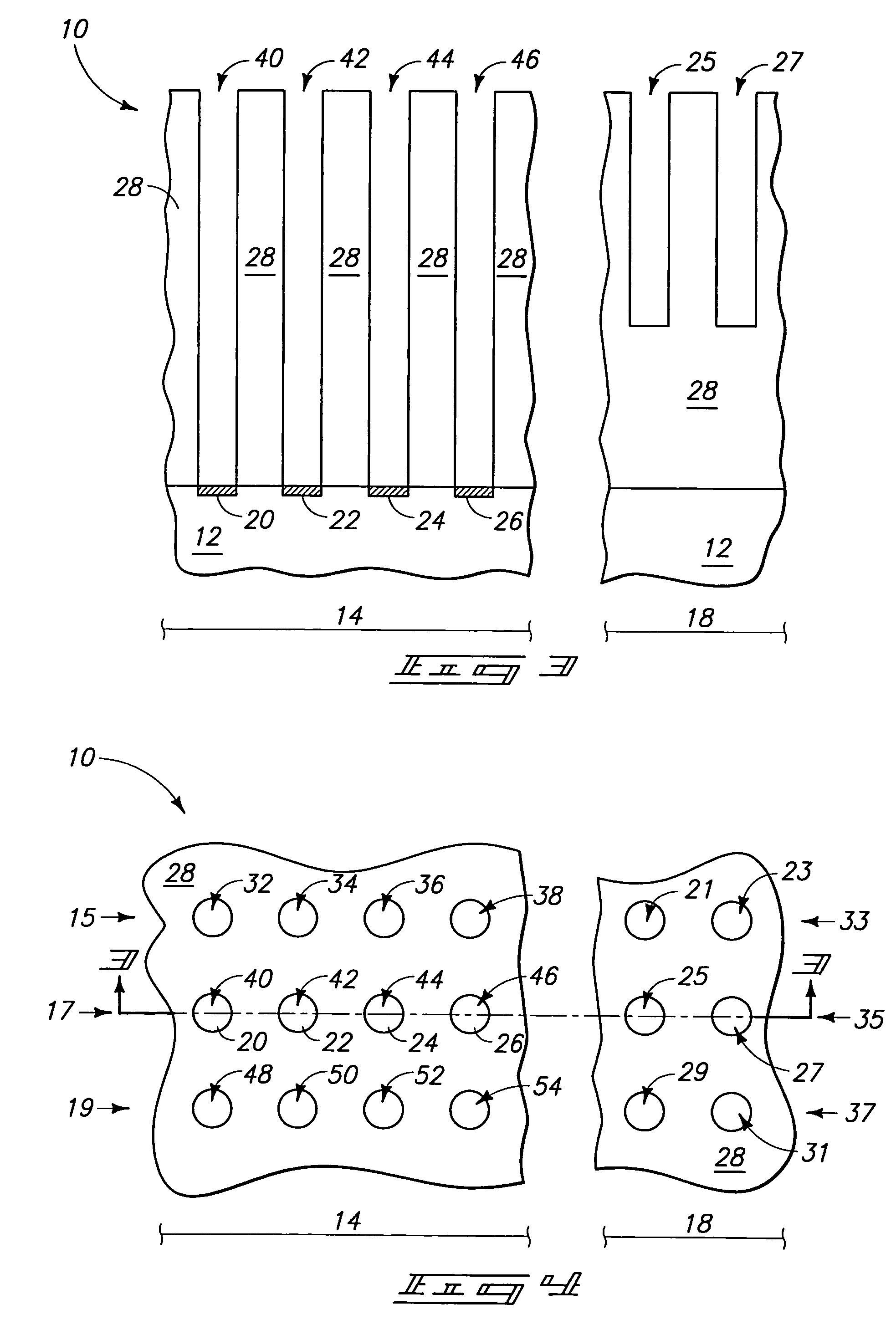
[0031]Referring to FIG. 1, a semiconductor substrate in process in accordance with an aspect of the invention is indicated generally with reference to numeral 10. Such comprises a substrate 12 which in one exemplary embodiment comprises a semiconductor substrate, for example comprised of bulk monocrystalline silicon or other material. In th...


PUM

PropertyMeasurementUnit
thicknessaaaaaaaaaa
thicknessaaaaaaaaaa
thicknessaaaaaaaaaa

Abstract

A plurality of capacitor electrode openings is formed within capacitor electrode-forming material. A first set of the openings is formed to a depth which is greater within the capacitor electrode-forming material than is a second set of the openings. Conductive first capacitor electrode material is formed therein. A sacrificial retaining structure is formed elevationally over both the first capacitor electrode material and the capacitor electrode-forming material, leaving some of the capacitor electrode-forming material exposed. With the retaining structure in place, at least some of the capacitor electrode-forming material is etched from the substrate effective to expose outer sidewall surfaces of the first capacitor electrode material. Then, the sacrificial retaining structure is removed from the substrate, and then capacitor dielectric material and conductive second capacitor electrode material are formed over the outer sidewall surfaces of the first capacitor electrode material formed within the first and second sets of capacitor openings.

Description

RELATED PATENT DATA[0001]This patent resulted from a continuation application of U.S. patent application Ser. No. 10 / 928,931, filed Aug. 27, 2004 now U.S. Pat. No. 7,202,127, entitled “Methods of Forming a Plurality of Capacitors”, naming Brett W. Busch, Fred D. Fishburn and James Rominger as inventors, the disclosure of which is incorporated by reference.TECHNICAL FIELD[0002]This invention relates to methods of forming a plurality of capacitors.BACKGROUND OF THE INVENTION[0003]Capacitors are one type of component which is commonly used in the fabrication of integrated circuit, for example in DRAM circuitry. A typical capacitor is comprised of two conductive electrodes separated by a non-conducting dielectric region. As integrated circuitry density has increased, there is a continuing challenge to maintain sufficiently high storage capacitance despite typical decreasing capacitor area. The increase in density of integrated circuitry has typically resulted in greater reduction in the...

Claims


Application Information

Patent Timeline
Patent Type & Authority Patents(United States)
IPC IPC(8): H01L21/8242
CPCD01F1/04D01F8/14D01F6/62Y10T428/2933
Inventor BUSCH, BRETT W.FISHBURN, FRED D.ROMINGER, JAMES
Owner ROUND ROCK RES LLC
Why Eureka
Try Eureka