
Semiconductor circuit arrangement for controlling a high voltage or a current of high current intensity

a technology of high current intensity and semiconductor, applied in the field of semiconductor circuit arrangement, can solve the problems of igbts' top side giving rise to technological disadvantages, failure of individual components during operation, and difficulty in using power semiconductor in high power ranges, etc., and achieve the effect of simple manner

Active Publication Date: 2008-11-11
INFINEON TECH AG
View PDF27 Cites 2 Cited by
  • Summary
  • Abstract
  • Description
  • Claims
  • Application Information

AI Technical Summary

Benefits of technology

The patent describes a semiconductor circuit arrangement for controlling high voltage and current. The arrangement includes multiple semiconductor modules, each containing components that can conduct or block voltage or current. The modules are designed so that when one component fails, the remaining components can automatically change into a blocking state to prevent the entire circuit from being affected. This ensures that the circuit can still function properly even if one of the modules fails. The arrangement can be used for controlling high voltage or current, and can be designed to have redundant components to ensure that the circuit can still control the voltage or current even if one of the modules fails.

Problems solved by technology

However, it is difficult to use power semiconductors in high power ranges on account of the limited dielectric strength and current-carrying strength.
Since a relatively large number of semiconductor components are used in series circuits of this type, the failure of individual components during operation must be expected.
However, the MOS structures (MOS=Metal Oxide Semiconductor) on the top side of the chip of IGBTs give rise to technological disadvantages.
The fabrication methods for IGBTs in presspack housings are therefore very complicated and expensive.
In this case, when a semiconductor module becomes conductive as a result of a functional disturbance, this results in the entire parallel circuit and thus the semiconductor circuit arrangement becoming conductive for the current.
In this case, it is thus not possible to operate with a component in the form of a presspack but rather, in the event of a functional disturbance, it must be ensured that the semiconductor module is isolated from the circuit arrangement or at least from the current path.

Method used


Image

  • Semiconductor circuit arrangement for controlling a high voltage or a current of high current intensity
  • Semiconductor circuit arrangement for controlling a high voltage or a current of high current intensity
  • Semiconductor circuit arrangement for controlling a high voltage or a current of high current intensity

Examples


Embodiment Construction

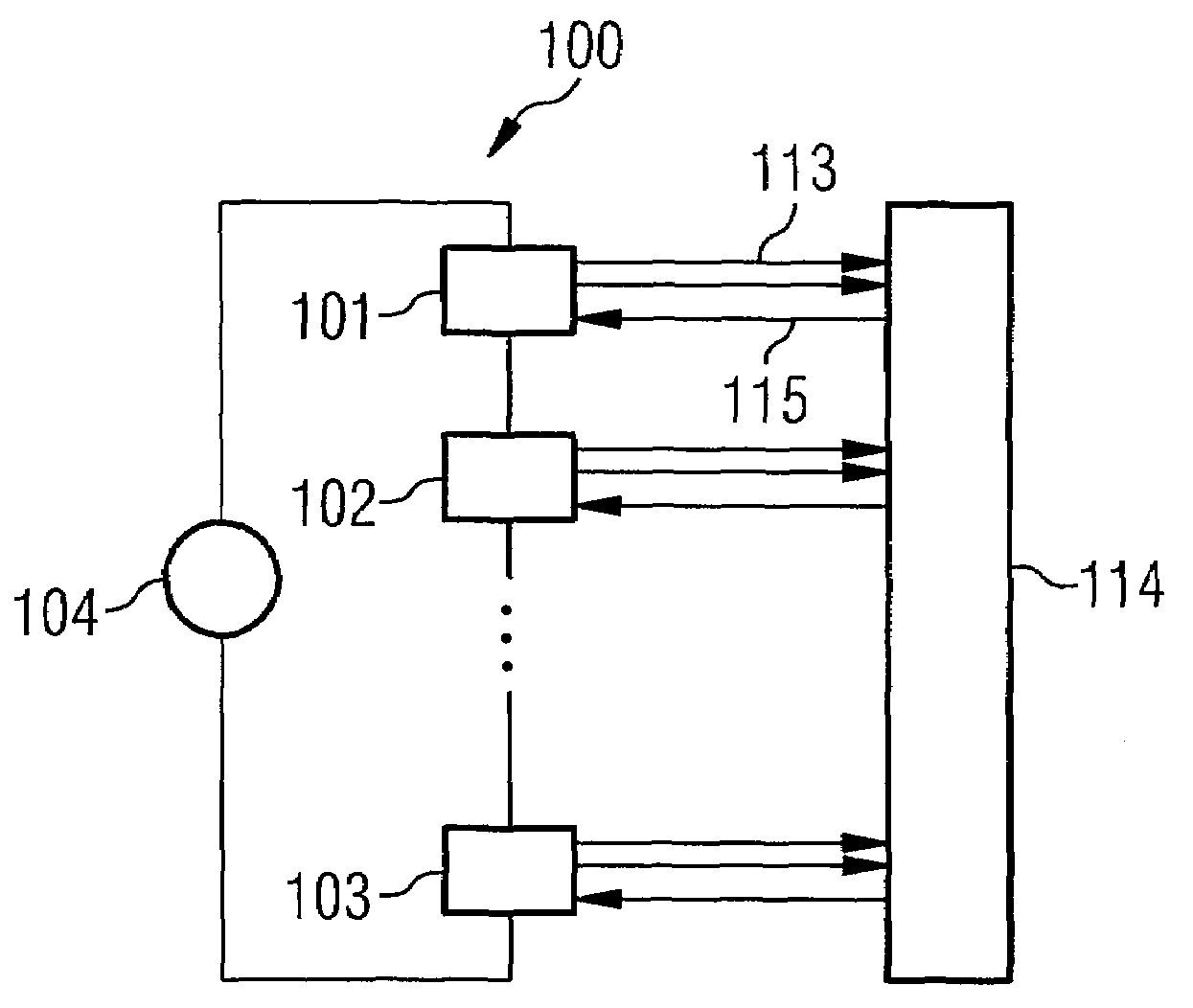
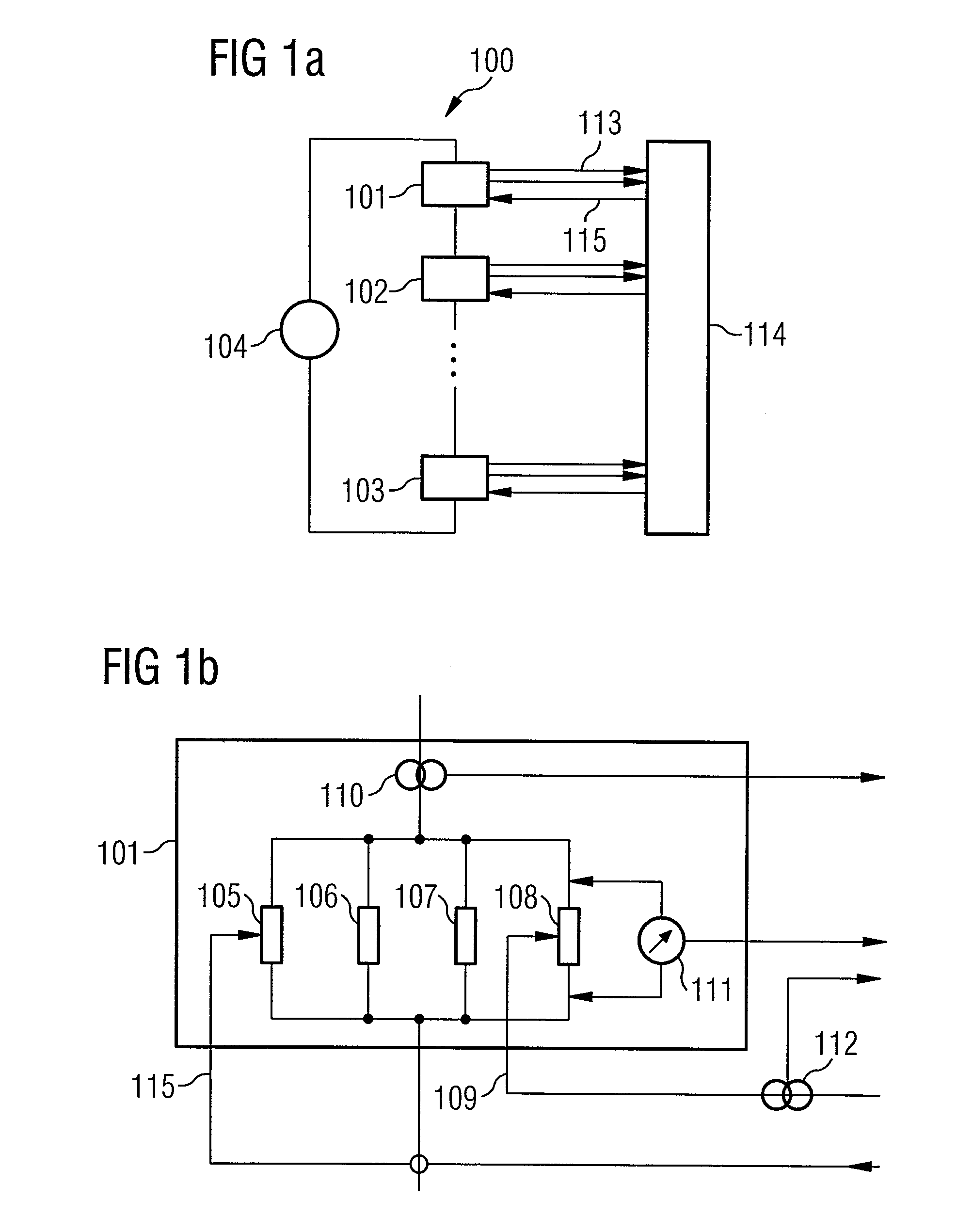
[0040]The semiconductor circuit arrangement 100 in accordance with FIG. 1a exhibits a series circuit of semiconductor modules 101, 102, 103, a high voltage that is symbolized by the voltage source 104 being applied to said series circuit. Partial voltages of the voltage 104 are respectively applied to each of the semiconductor modules 101, 102, 103.

[0041]As FIG. 1b shows, each of the semiconductor modules 101, 102, 103 (of which only one, 101, is illustrated by way of example) comprises, inter alia, a parallel circuit of components 105, 106, 107, 108, each individual one of which can block or conduct the voltage applied to the semiconductor module 101. Each of the components has a control input, which is illustrated merely by way of example in the components 105, 108 by means of the lead 109, 115 and which is driven by a control device. During normal operation, the components 105, 106, 107, for example, may be permanently driven in a blocking manner and, depending on the requirement...


PUM


Abstract

In the case of a semiconductor circuit arrangement for controlling a high voltage with a series circuit of semiconductor modules, the high voltage possibly being dropped between the ends of the series circuit, increased functional reliability is achieved by each semiconductor module having a parallel circuit of at least two components, at least one first component of which can be conducting or blocking, during normal operation, for that partial voltage of the high voltage which is applied to it, by the remaining component(s) of a parallel circuit blocking, during normal operation, at least when the first component blocks, and by each semiconductor module being set up in such a manner that, in the event of a functional disturbance in the first component, the remaining component(s) permanently change(s) into a conducting state.

Description

CROSS REFERENCE TO RELATED APPLICATION[0001]This application is a continuation of copending International Application No. PCT / EP03 / 11757 filed Oct. 23, 2003 which designates the United States, and claims priority to German application no. 102 55 602.4 filed Nov. 28, 2002.TECHNICAL FIELD OF THE INVENTION[0002]The invention relates to a semiconductor circuit arrangement for controlling a high voltage with a series circuit of semiconductor modules, the high voltage possibly being dropped between the ends of the series circuit.[0003]In addition, the invention relates to a semiconductor circuit arrangement for controlling a current of high current intensity with a parallel circuit of semiconductor modules which each carry partial currents.BACKGROUND OF THE INVENTION[0004]The invention is used in technical fields in which power semiconductors are used to control high voltages, typically at least several thousand volts, or high currents, typically at least several hundred amperes. This is ...

Claims


Application Information

Patent Timeline
Patent Type & Authority Patents(United States)
IPC IPC(8): H01H79/00H03K17/10H03K17/12
CPCH03K17/107H03K17/122H01L2224/48091H01L2924/00014
Inventor BAYERER, REINHOLD
Owner INFINEON TECH AG
Learn More