Solid-state image sensing device

a sensing device and solid-state technology, applied in the direction of radio frequency controlled devices, transistors, television systems, etc., can solve the problems of high power consumption and high drive voltage of ccds, high cost, and inability to produce through ordinary semiconductor manufacturing processes, so as to improve the light shielding capability of floating diffusion portions

Inactive Publication Date: 2008-11-25
CANON KK
View PDF22 Cites 21 Cited by
  • Summary
  • Abstract
  • Description
  • Claims
  • Application Information

AI Technical Summary

Benefits of technology

[0018]The present invention has been made in light of the above-described situation, and has as its object to improve the light-shielding capability of the floating diffusion portion of a MOS-type solid-state image sensing device.

Problems solved by technology

On the other hand, however, CCDs have high power consumption and high drive voltages, and moreover, cannot be produced through the ordinary semiconductor manufacture process and are therefore expensive.
Furthermore, a problem with CCDs is that it is difficult to integrate the drive circuitry and other peripheral circuits.
However, with the conventional CMOS-type solid-state image sensing device described above, signal electrons generated in response to incoming light causes the output voltage to fluctuate.
However, although the structure described in Japanese Patent Application Laid-Open No. 2000-124438 can shield an area except for the aperture from light, it does so at the cost of performing the extremely difficult process of leaving the light-shielding member only at the side surfaces of fine pixels.
Consequently, the actual aperture is extremely narrow, which reduces sensitivity and is thus not a practical solution.

Method used


Image

  • Solid-state image sensing device
  • Solid-state image sensing device
  • Solid-state image sensing device

Examples


first embodiment

[0047]A detailed description will now be given of the structure of the pixels of a solid-state image sensing device according to a first embodiment of the present invention, used in an image sensing device and the like having the structure described above.

[0048]FIG. 4 is a diagram showing the layout of a pixel circuit of a first embodiment of the present invention. It should be noted that elements that are identical to those shown in FIG. 12 are assigned the same reference characters and a description thereof is omitted.

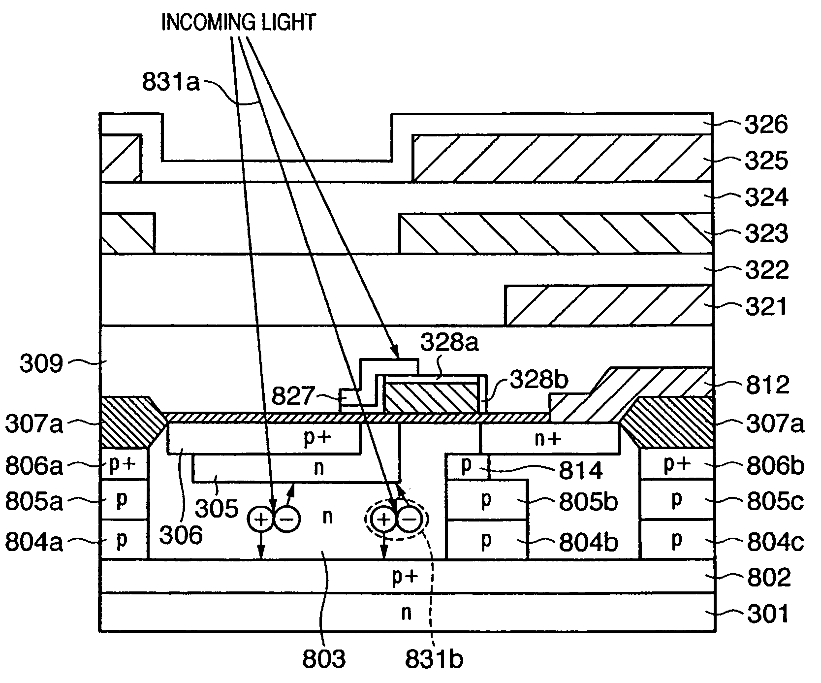
[0049]In FIG. 4, reference numeral 73 indicates a light-shielding member of the gate electrode of the transfer MOS transistor 2. The light-shielding member 73 shields the polysilicon of the gate electrode of the transfer MOS transistor 2 so as to cover the polysilicon 21 with respect to the direction of the length of the channel, and is slightly larger than the width of the channel so as to prevent incoming light from entering directly beneath the FD portion 3. Below...

second embodiment

[0058]FIG. 6 is a diagram showing an example of a pixel of a MOS-type solid-state image sensing device according to a second embodiment of the present invention, viewed in cross-section. In FIG. 6, elements that are identical to those of the first embodiment described above using FIG. 5 are assigned the same reference characters and a description thereof is omitted.

[0059]As shown in FIG. 6, the shapes of light-shielding members 427a, 427b of the second embodiment are different from the shapes of the light-shielding members 327a, 327b of the first embodiment shown in FIG. 5. In this second embodiment as well, the light-shielding members 427a, 427b are disposed so as to cover the top of the gate electrode 304 through thin the silicon oxide films 328a, 328b. However, although the side and the top of the side of the gate electrode 304 that faces the PD 1 is covered by the light-shielding members 427a, 427b, the top and the side of the side that faces the FD portion 3 is not covered by a...

third embodiment

[0062]FIG. 7 is a diagram showing an example of a pixel of a MOS-type solid-state image sensing device according to a third embodiment of the present invention, viewed in cross-section. In FIG. 7, elements that are identical to those of the first embodiment described above using FIG. 5 are assigned the same reference characters and a description thereof is omitted.

[0063]In the third embodiment, there is no thin silicon oxide film 328a covering the top of the gate electrode 304 as shown in FIG. 6 in the asymmetrical light-shielding members 427a, 427b of the second embodiment. In addition, shown in the diagram is an example in which the gate electrode 304 and the light-shielding members 527a, 527b contact each other directly along the top and the side of the gate electrode 304.

[0064]With the third embodiment, as shown in FIG. 7 the light-shielding members 527a, 527b are made of two layers of metal, with a barrier metal used for one layer 527b directly contacting the gate electrode 304...


PUM


Abstract

A solid-state image sensing device has a pixel that includes a photodiode that generates an electrical charge according to an amount of incoming light, a floating diffusion portion, a charge transfer transistor that transfers the electrical charge to the floating diffusion portion from the photoelectric conversion portion, a reading circuit that outputs an signal on the basis of said electrical charge held in said floating diffusion portion, and a light-shielding member disposed so as to cover a side wall of a gate electrode of the charge transfer transistor on the photoelectric conversion portion side.

Description

FIELD OF THE INVENTION[0001]The present invention relates to solid-state image sensing device, and more particularly, to a MOS-type solid-state image sensing device.BACKGROUND OF THE INVENTION[0002]In recent years, demand has increased rapidly for solid-state image sensing devices used as image sensing devices for image input mainly in digital still cameras and video cameras.[0003]For these types of solid-state image sensing devices, CCD and MOS-type image sensors are widely used. The former are widely used as high picture quality image sensing devices due to their higher sensitivity and lower noise than the latter. On the other hand, however, CCDs have high power consumption and high drive voltages, and moreover, cannot be produced through the ordinary semiconductor manufacture process and are therefore expensive. Furthermore, a problem with CCDs is that it is difficult to integrate the drive circuitry and other peripheral circuits. By contrast, MOS-type image sensors can make up f...

Claims


Application Information

Patent Timeline
Patent Type & Authority Patents(United States)
IPC IPC(8): H01L31/062H01L27/14H01L27/146H04N5/335H04N5/355H04N5/361H04N5/369H04N5/372
CPCH01L27/14612H01L27/14623
Inventor INOUE, SHUNSUKE
Owner CANON KK
Why Eureka
Try Eureka