Method for producing an optical device, optical device, image display apparatus, and head-mounted display

a technology of optical devices and head-mounted displays, applied in the direction of instruments, holographic processes, holographic nature/properties, etc., can solve problems such as inability to obtain, and achieve the effects of reducing power consumption, reducing current amounts, and reducing brightness

Active Publication Date: 2008-12-02
KONICA MINOLTA PHOTO IMAGING
View PDF4 Cites 14 Cited by
  • Summary
  • Abstract
  • Description
  • Claims
  • Application Information

AI Technical Summary

Benefits of technology

[0015]In this way, consideration is given to the light intensity at the individual diffraction peak wavelengths of the light from the reproduction light source actually used, and the exposure amounts of laser light at the different wavelengths are so adjusted as to obtain diffraction efficiency commensurate with the light intensity. Then, with the so adjusted exposure amounts, the optical element is formed on the transparent base member. This makes it possible to adjust the hue of the light (reproduction light) obtained from the reproduction light source via the optical element to the one desired with every reproduction light source used, while the most use is made of the light emitted from the reproduction light source actually used. Thus, it is possible to obtain, with every reproduction light source used, a bright image with a good color balance.
[0016]According to another aspect of the present invention, a method for producing an optical device includes: a bonding step of bonding a hologram photosensitive material on a transparent base member; and an exposing step of exposing the hologram photosensitive material to laser light of a plurality of different wavelengths from a fabrication light source in order to form on the transparent base member a hologram optical element having diffraction efficiency peaks at a plurality of diffraction peak wavelengths corresponding to the plurality of different wavelengths. Here, the exposing step includes a step of adjusting the exposure amounts of laser light of the different wavelengths from the fabrication light source in such a way that, when a plurality of illumination light sources corresponding to the individual diffraction peak wavelengths are used as a reproduction light source during reproduction, the diffraction efficiency at the diffraction peak wavelength corresponding to, of the plurality of illumination light sources, the illumination light source that consumes the least electric power when fed with a given amount of current is lower than the diffraction efficiency at the other diffraction peak wavelengths.
[0020]By contrast, with the design described above, for example, the diffraction efficiency at the diffraction peak wavelengths G1 and B1 corresponding to the G and B illumination light sources, which consume more electric power than the R illumination light source, is set to be higher than at the diffraction peak wavelength R1. This makes it possible, without reducing the amounts of R, G, and B light ultimately obtained, to reduce the amounts of current fed to the G and B illumination light sources and thereby reduce their power consumption. That is, it is possible to obtain the same brightness while saving electric power.
[0021]Moreover, since the diffraction efficiency at the diffraction peak wavelength R1 corresponding to the R illumination light source, which consumes the least electric power, is set to be lower than at the other diffraction peak wavelengths G1 and B1, it is possible to increase the amount of current fed to the R illumination light source and thereby increase the amount of light emitted therefrom within the range of the prescribed sum of power consumption. Incidentally, when fed with a given current, the R illumination light source consumes the least electric power, and therefore the rate (variation rate) at which power consumption increases in response to an increase in current is the lowest with the R illumination light source. This makes it possible to obtain bright light while saving power as much as possible.
[0023]That is, with the design described above, it is possible not simply to obtain, with every reproduction light source used, a bright image with a good color balance but simultaneously to achieve power saving in the reproduction light source.

Problems solved by technology

That is, inconveniently, it is impossible to obtain, with every reproduction light source used, a bright image with a good color balance.

Method used


Image

  • Method for producing an optical device, optical device, image display apparatus, and head-mounted display
  • Method for producing an optical device, optical device, image display apparatus, and head-mounted display
  • Method for producing an optical device, optical device, image display apparatus, and head-mounted display

Examples


Embodiment Construction

[0059]Hereinafter, an embodiment of the present invention will be described with reference to the drawings.

1. Head-Mounted Display

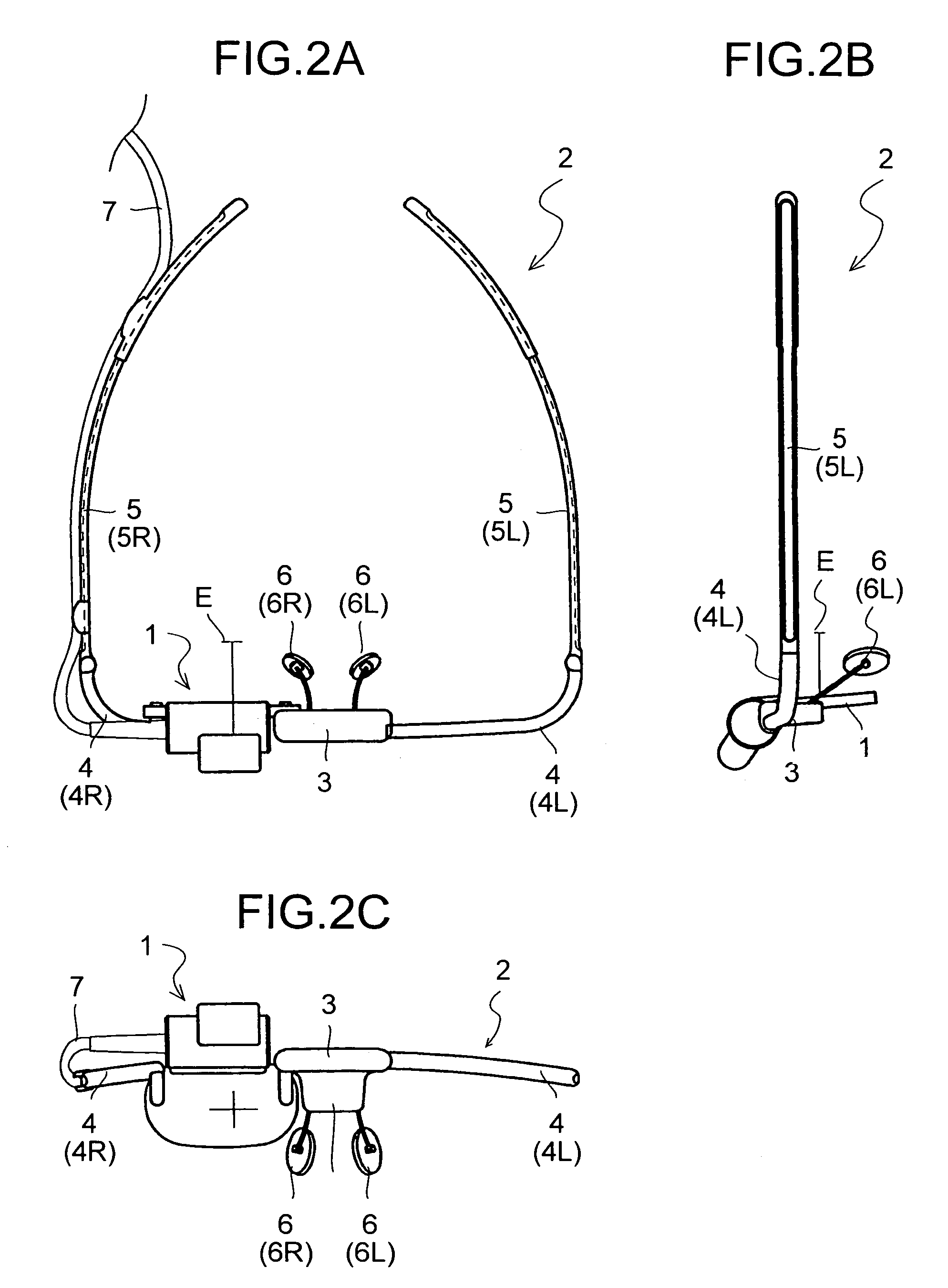
[0060]FIG. 2A is a plan view showing an outline of the structure of a head-mounted display (hereinafter abbreviated to “HMD”) embodying the invention, FIG. 2B is a side view of the same HMD, and FIG. 2C is a front view of the same HMD. The HMD includes an image display apparatus 1 and a supporter 2 that supports it, and has an appearance like that of common eyeglasses of which one of the lenses (for example, the left-eye lens) has been removed.

[0061]The image display apparatus 1 permits an observer to observe the outside-world image in a see-through fashion, and simultaneously displays an image to feed it, as a virtual image, to the observer. In the image display apparatus 1 shown in FIG. 2C, the part thereof that corresponds to the right-eye lens of eyeglasses is composed of two transparent base members 22 and 23 (see FIG. 4), which will be described lat...


PUM


Abstract

The exposure amounts of R, G, and B laser light emitted from a fabrication light source are so adjusted that the diffraction efficiency at R, G, and B wavelengths in an optical element is commensurate with the light intensity at the R, G, and B wavelengths in the light emitted from a reproduction light source. For example, when the light intensity of the light emitted from the reproduction light source is increasingly low at the B, G, and R wavelengths in this order, the exposure amounts of the R, G, B, laser light emitted from the fabrication light source are so adjusted that the diffraction efficiency in the optical element is increasingly high at the B, G, and R wavelengths in this order. In this way, the hue of the light (reproduction light) obtained from the reproduction light source via the optical element can be adjusted to the hue desired with every reproduction light source used, while the most use is made of the light emitted from the reproduction light source actually used.

Description

[0001]This application is based on Japanese Patent Application No. 2004-351731 filed on Dec. 3, 2004 and Japanese Patent Application No. 2005-302597 filed on Oct. 18, 2005, the contents of both of which are hereby incorporated by reference.BACKGROUND OF THE INVENTION[0002]1. Field of the Invention[0003]The present invention relates to a method for producing an optical device having an optical element formed as a hologram on a transparent base member, to such an optical device, to an image display apparatus employing such an optical device, and to a head-mounted display employing such an image display apparatus.[0004]2. Description of Related Art[0005]When used embedded in a transparent base member, an optical element such as a hologram, half-mirror coat, or beam splitter layer is immune to ambient conditions such as humidity and the presence of oxygen. This makes such an optical element useful as a combiner in, for example, a head-up display or head-mounted display.[0006]In particul...

Claims


Application Information

Patent Timeline
Patent Type & Authority Patents(United States)
IPC IPC(8): G03H1/02
CPCG02B5/32G02B27/0172G02B2027/0109G02B2027/0132G02B2027/0174G02B2027/0178G03H2222/18G03H2240/52
Inventor NODA, TETSUYAKASAI, ICHIROENDO, TAKESHITANIJIRI, YASUSHI
Owner KONICA MINOLTA PHOTO IMAGING
Why Eureka
Try Eureka