Methods for designing, evaluating and manufacturing semiconductor devices

a technology for semiconductor devices and manufacturing methods, applied in the direction of cad circuit design, program control, instruments, etc., can solve the problems of reducing the production yield of semiconductor devices, unstable operation of semiconductor devices in long-term use, and generating electromigration. , to achieve the effect of improving accuracy and evaluating the reliability of semiconductor devices

Inactive Publication Date: 2008-12-09
RENESAS ELECTRONICS CORP
View PDF10 Cites 12 Cited by
  • Summary
  • Abstract
  • Description
  • Claims
  • Application Information

AI Technical Summary

Benefits of technology

[0010]A present inventors have had an assumption that a coupling failure between the copper interconnect and the via is occurred, when the growing region of the void growing from an origin in the copper interconnect expands to the entire contacting region between the copper interconnect and the via. The growing region of the void expands over time. On the contrary, the contacting region between the copper interconnect and the via is determined by the geometric factor of the via. Since the geometric factor of the via is determined in the light of the anticipated value xopen of the dimension of the growing region of the void expanding in the desired stress induced voiding (SIV)-ensured time topen according to the present invention, the coupling failure between the copper interconnect and the via occurred in the SIV-ensured time topen can be prevented. This allows designing the semiconductor device having the desired reliability.
[0011]For example, the determining the geometric factor of the via according to the above aspect of the present invention may include determining the geometric factor of the via so that the dimension of the contacting region is not smaller than the anticipated value xopen. This prevents causing the coupling failure between the copper interconnect and the via in the SIV-ensured time topen.
[0014]According to the present invention, the SIV-ensured time topen can be calculated by comparing the anticipated value x of the growing region of the void with the dimension of the contacting region between the copper interconnect and the via, calculated on the basis of the geometric factor of the via. Having this configuration, the SIV-ensured time topen can be calculated with an improved accuracy, without a need for conducting the time-consuming SIV test. Having this configuration, the evaluation on the reliability of the semiconductor device can be simply conducted with an improved accuracy.
[0017]According to the present invention, a semiconductor device having a desired reliability can be designed. In addition, according to the present invention, reliability of a semiconductor device can be evaluated with an improved accuracy without a need for conducting a time-consuming test.

Problems solved by technology

On the contrary, the generation of electromigration has become a problem in such type of the interconnect made of copper. FIG. 17 is a schematic cross sectional view of a copper multiple-layered interconnect formed via a damascene process.
This causes problems of a reduction in a production yield of semiconductor devices or an unstable operation of semiconductor device in the long term use.
H7-235,596, a barrier metal film of the via comes in contact with a barrier metal film of the lower layer interconnect, leading to a problem of an increased interconnect resistance.
In particular, when the void is generated between the side wall of the via and the lower layer interconnect, the configuration including the electrical coupling between the barrier metal films exhibits unwanted higher resistance.
Once such situation is attained, it is impossible to maintain lower resistance even if copper is employed for the interconnect material.

Method used


Image

  • Methods for designing, evaluating and manufacturing semiconductor devices
  • Methods for designing, evaluating and manufacturing semiconductor devices
  • Methods for designing, evaluating and manufacturing semiconductor devices

Examples


first embodiment

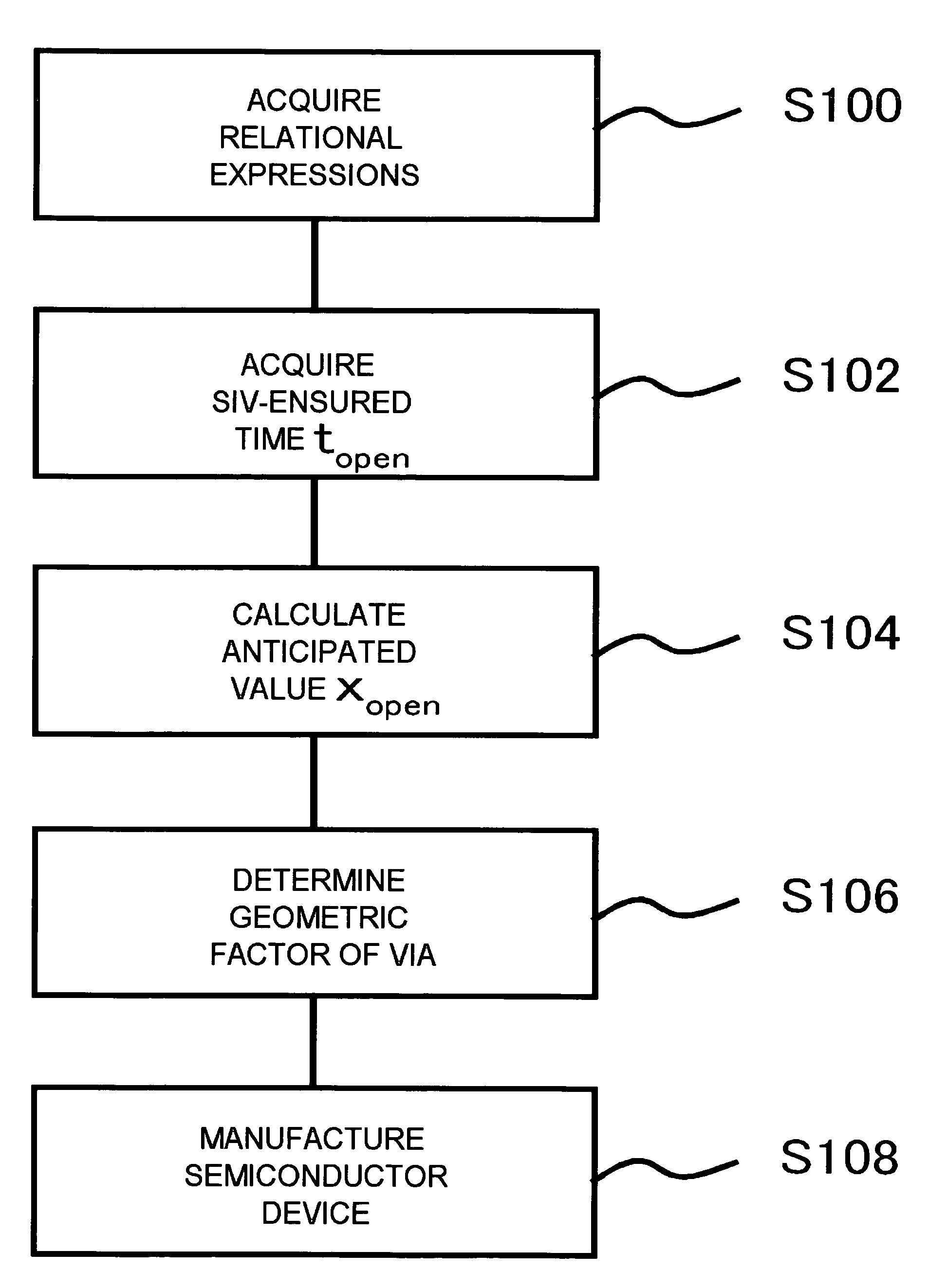
[0065]FIG. 10 is a flow chart, showing a procedure of designing the semiconductor device 100 in the present embodiment.

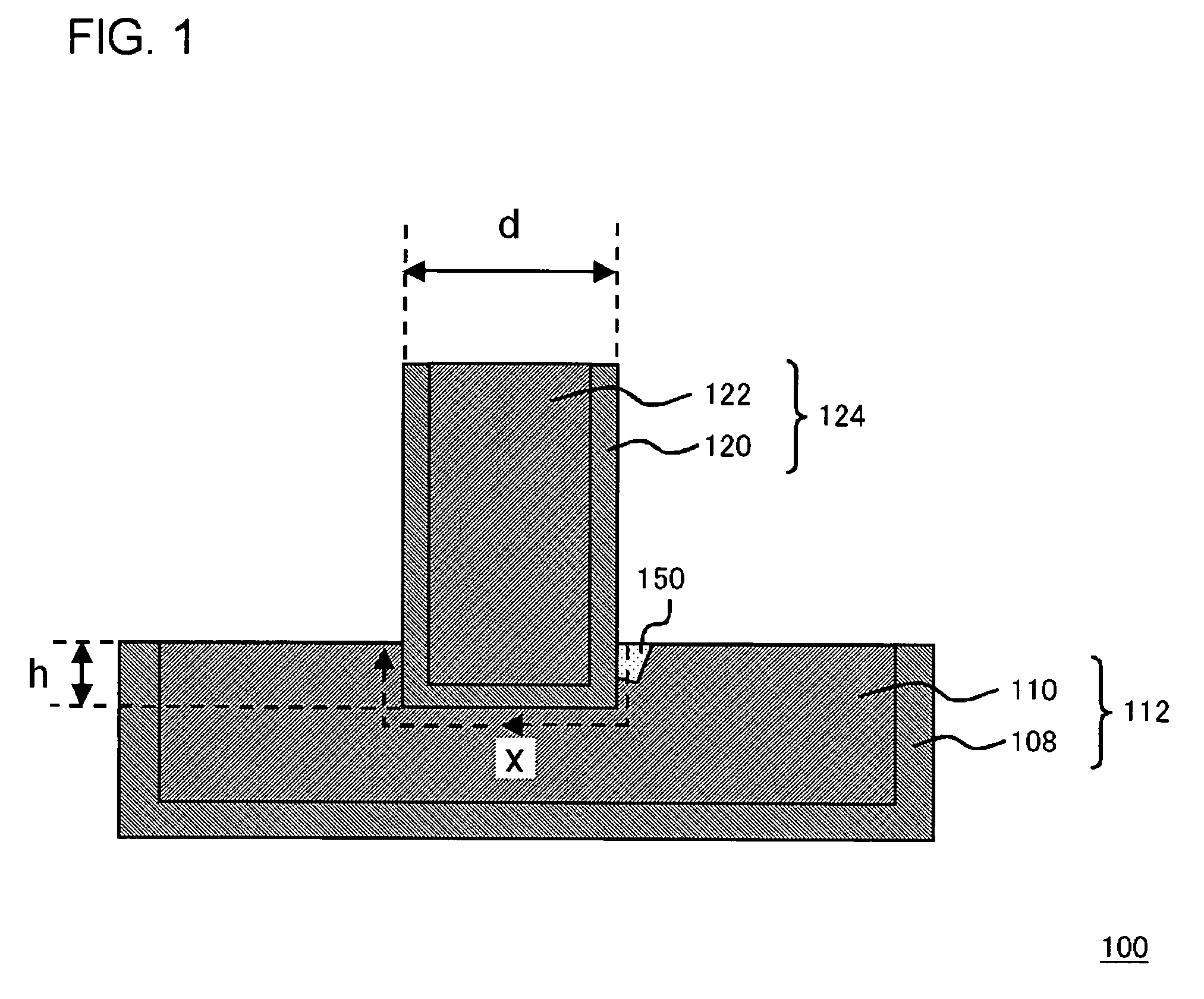
[0066]First, relational expressions shown in formula 11 and formula 12 are acquired (S100). Subsequently, a target SIV-ensured time topen is acquired (S102). Then, topen acquired in step S102 is substituted into the relational expressions to acquire an anticipated value xopen (S104). Here, values of stress S and / or Cu / area ratio σ can be controlled by appropriately controlling the conditions for manufacturing the semiconductor device. The interconnect parameters are determined by the conditions for manufacturing the semiconductor device. The interconnect parameters are substituted into formula 11 or formula 12 to obtain the anticipated value xopen. Subsequently, a geometric factor of the via is determined based on the anticipated value xopen (S106). For example, a geometric factor of the via is determined so as to satisfy the relationship of: d+2 h≧anticipated val...

second embodiment

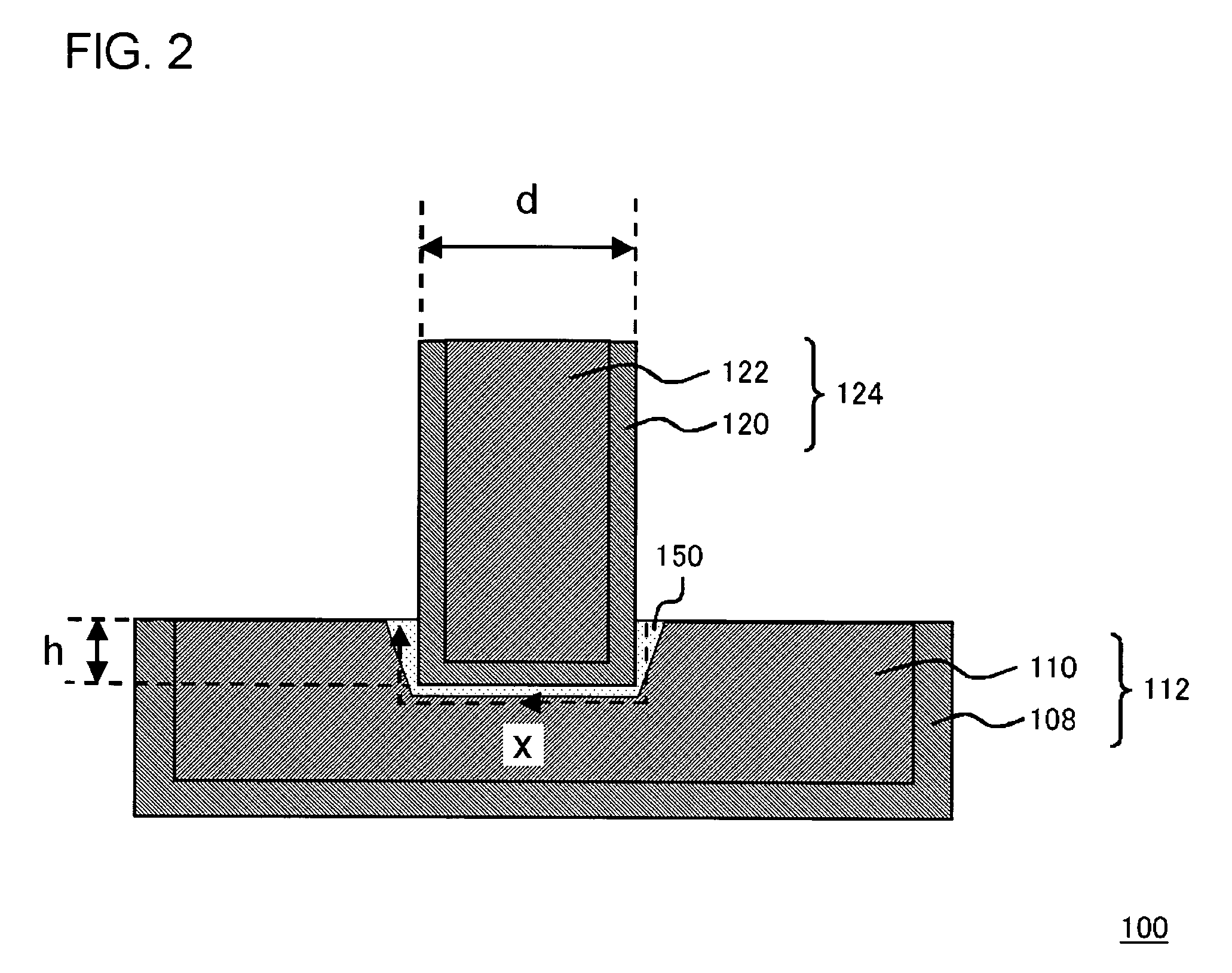
[0084]FIG. 15 is a flow chart, showing a procedure for calculating the SIV-ensured time topen in the present embodiment. First, relational expressions shown in formula 11 and formula 12 are acquired (S200). Subsequently, an anticipated value xopen is calculated based on characteristics of the via geometry of the semiconductor device to be manufactured (S202). Here, the anticipated value xopen is calculated so as to satisfy the relationship of: anticipated value xopen≦d+2 h, for example. Then, the anticipated value xopen and the interconnect parameters are substituted into the relational expressions to obtain the calculated result of the SIV-ensured time topen (S204). Here, values of stress S and / or Cu / area ratio σ can be controlled by appropriately controlling the conditions for manufacturing the semiconductor device. The interconnect parameters are determined by the conditions for manufacturing the semiconductor device.

[0085]For example, in the interconnect structure shown in FIG....

third embodiment

[0088]In the present embodiment, configurations of systems for conducting a process for calculating a geometric factor of a via described in first embodiment and a process for calculating an SIV-ensured time topen described in second embodiment will be described.

[0089]FIG. 16 is a block diagram, showing a configuration of designing / evaluating apparatus 200. The designing / evaluating apparatus 200 include an input accepting unit 202, a correction processing unit 204, a calculation processing unit 206, a relational expression storage unit 212 and an output processing unit 214. The calculation processing unit 206 include a geometric factor calculating unit 208 and an SIV-ensured time calculating unit 210.

[0090]The relational expression storage unit 212 stores the relational expressions presented in formula 11 and formula 12 and / or values of the interconnect parameters in a certain manufacturing condition. The input accepting unit 202 accepts an indication from a user.

[0091]Functions in ...


PUM


Abstract

A semiconductor device 100 has a configuration having a via 124 formed on a first interconnect 112. A method for designing the semiconductor device 100 includes: calculating an anticipated value xopen of a dimension of a growing region of a void 150 expanding in a stress induced voiding (SIV)-ensured time topen at a predetermined temperature, assuming that the void 150 grows from an origin in a copper interconnect (interconnect metallic film 110); and determining a geometric factor of the via 124 by comparing a dimension of a contacting region between a first interconnect 112 and the via 124 with the anticipated value xopen. The dimension of the contacting region may be presented as d+h (where d represents a diameter of a via 124, and h represents a buried depth that the via 124 is buried within the first interconnect 112).

Description

[0001]This application is based on Japanese Patent Application NO. 2005-002,277, the content of which is incorporated hereinto by reference.BACKGROUND[0002]1. Technical Field[0003]The present invention relates to a method for designing a semiconductor device, and to a method for evaluating reliability thereof.[0004]2. Related Art[0005]In recent years, for the purpose of satisfying the increasing requirements for achieving higher level of integration in a semiconductor device, copper becomes to be widely utilized for a material of interconnect lines or plugs. Copper is a material, which is characterized in having a lower resistance and a better electromigration resistance than that of aluminum that has been conventionally employed.[0006]On the contrary, the generation of electromigration has become a problem in such type of the interconnect made of copper. FIG. 17 is a schematic cross sectional view of a copper multiple-layered interconnect formed via a damascene process. The copper ...

Claims


Application Information

Patent Timeline
Patent Type & Authority Patents(United States)
IPC IPC(8): G06F9/45H01L21/4763H01L29/40H01L21/02H01L21/768H01L23/522
CPCG06F17/5068G06F30/39
Inventor ITOH, SATOSHI
Owner RENESAS ELECTRONICS CORP
Why Eureka
Try Eureka