
Clamp circuit with fuse options

a technology of fuse options and clamp circuits, which is applied in the direction of electric variable regulation, process and machine control, instruments, etc., can solve the problems of limited maximum supply voltage and damage to semiconductor devices

Inactive Publication Date: 2008-12-23
MICRON TECH INC
View PDF9 Cites 2 Cited by
  • Summary
  • Abstract
  • Description
  • Claims
  • Application Information

AI Technical Summary

Benefits of technology

The present invention relates to a voltage control circuit for semiconductor devices that limits the supply voltage during testing and after certification. The circuit uses fuses to limit the maximum supply voltage to a non-harmful level. The circuit includes a clamp circuit with voltage regulation devices that control a clamping threshold. A charge pump generates the test supply voltage based on the clamping threshold. A bypass device is activated after certification to lower the clamping threshold and generate the operational supply voltage. The method includes providing a plurality of voltage control elements, establishing a first voltage control signal, and generating the first supply voltage. The method also includes bypassing at least one voltage control element and establishing a second voltage control signal to generate the second supply voltage. The voltage control circuit and method limit the voltage level of the supply voltage to prevent damage to the semiconductor device during testing and ensure reliable operation.

Problems solved by technology

The maximum supply voltage available during testing is high enough to cause damage to the semiconductor device if the voltage is applied under non-controlled conditions.
After the manufacturer's testing is completed, the maximum supply voltage is limited by blowing fuses to bypass some of the voltage regulation devices.

Method used


Image

  • Clamp circuit with fuse options
  • Clamp circuit with fuse options
  • Clamp circuit with fuse options

Examples


Embodiment Construction

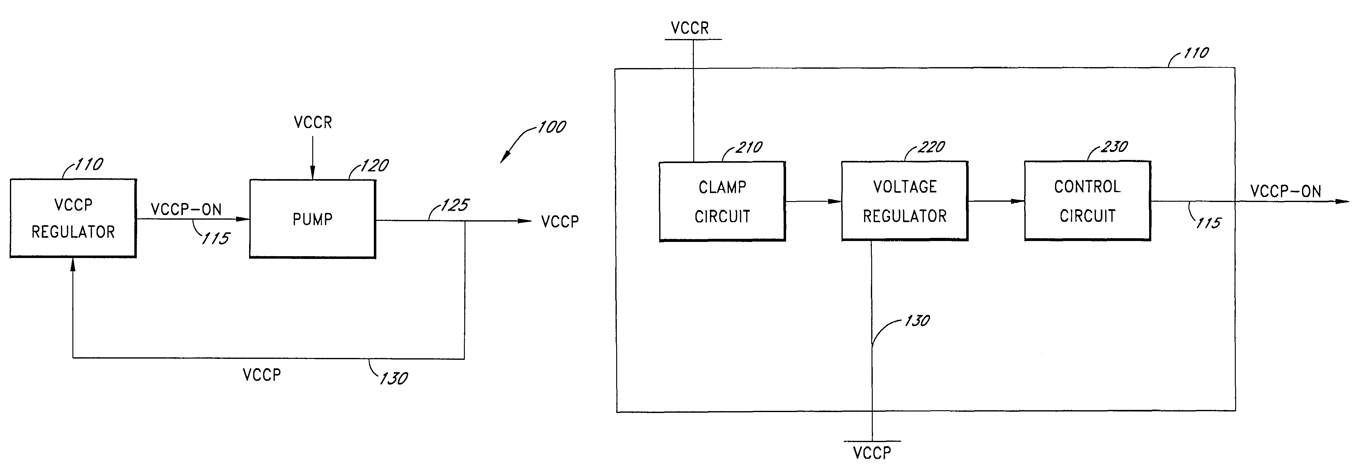
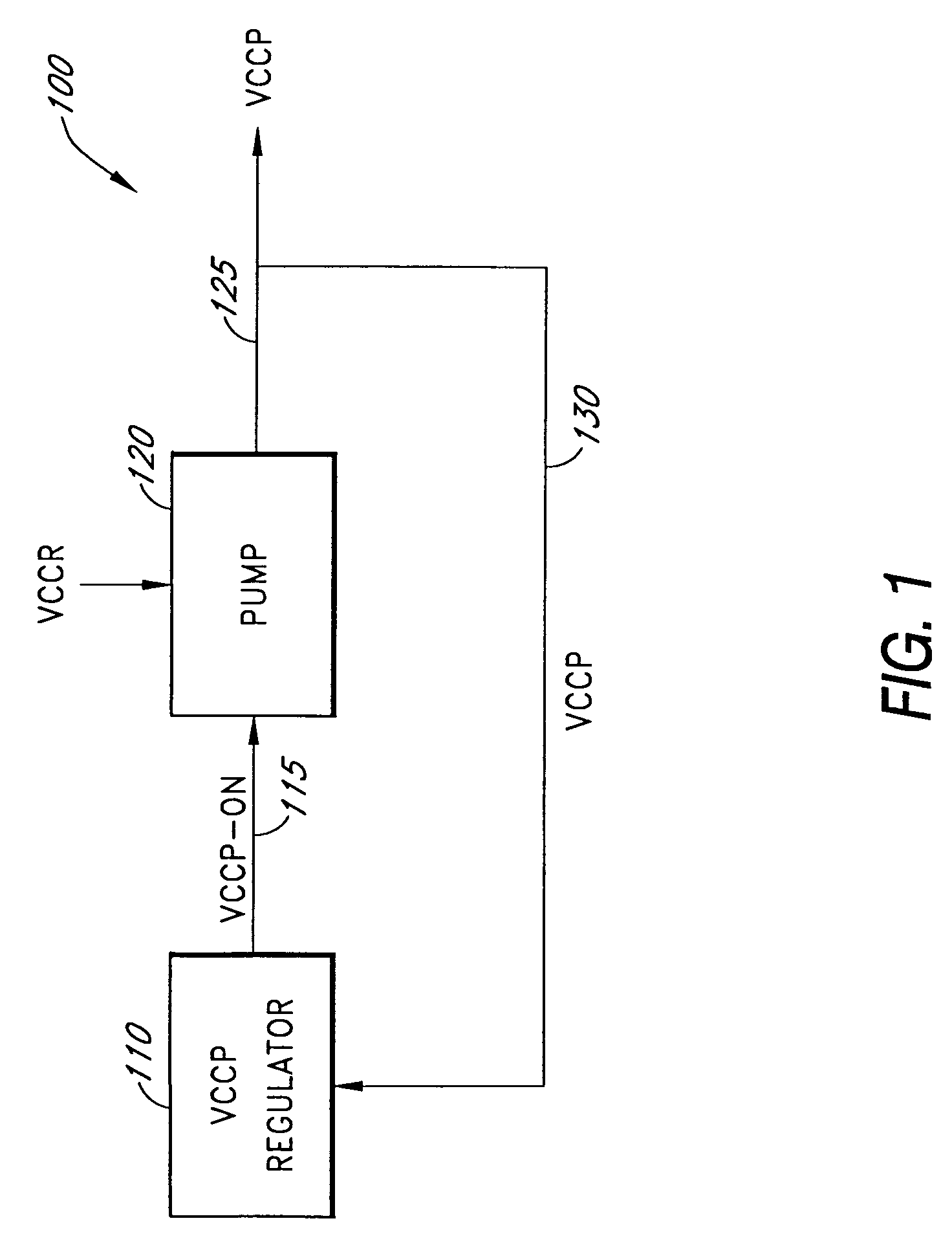
[0023]FIG. 1 is a block diagram illustrating a voltage control circuit 100 according to the present invention. The voltage control circuit 100 includes a VCCP regulator 110, a charge pump 120, and a feedback signal line 130. The VCCP regulator 110 generates an output signal VCCP-ON 115 which controls the charge pump 120. The charge pump 120 receives two inputs, a regulated voltage VCCR and the output signal VCCP-ON from the VCCP regulator 110. The output 125 of the charge pump 120 is the voltage VCCP. The voltage VCCP is fed back to as input to the VCCP regulator by the feedback signal line 130.

[0024]The value of the signal VCCP-ON 115 controls the operation of the charge pump 120. When VCCP is below the desired level, the signal VCCP-ON 115 causes the charge pump 120 to turn on, thereby increasing the value of VCCP. When VCCP is above the desired level, the signal VCCP-ON causes the charge pump 120 to turn off, thereby decreasing the value of VCCP. The charge pump 120 generates VCC...


PUM


Abstract

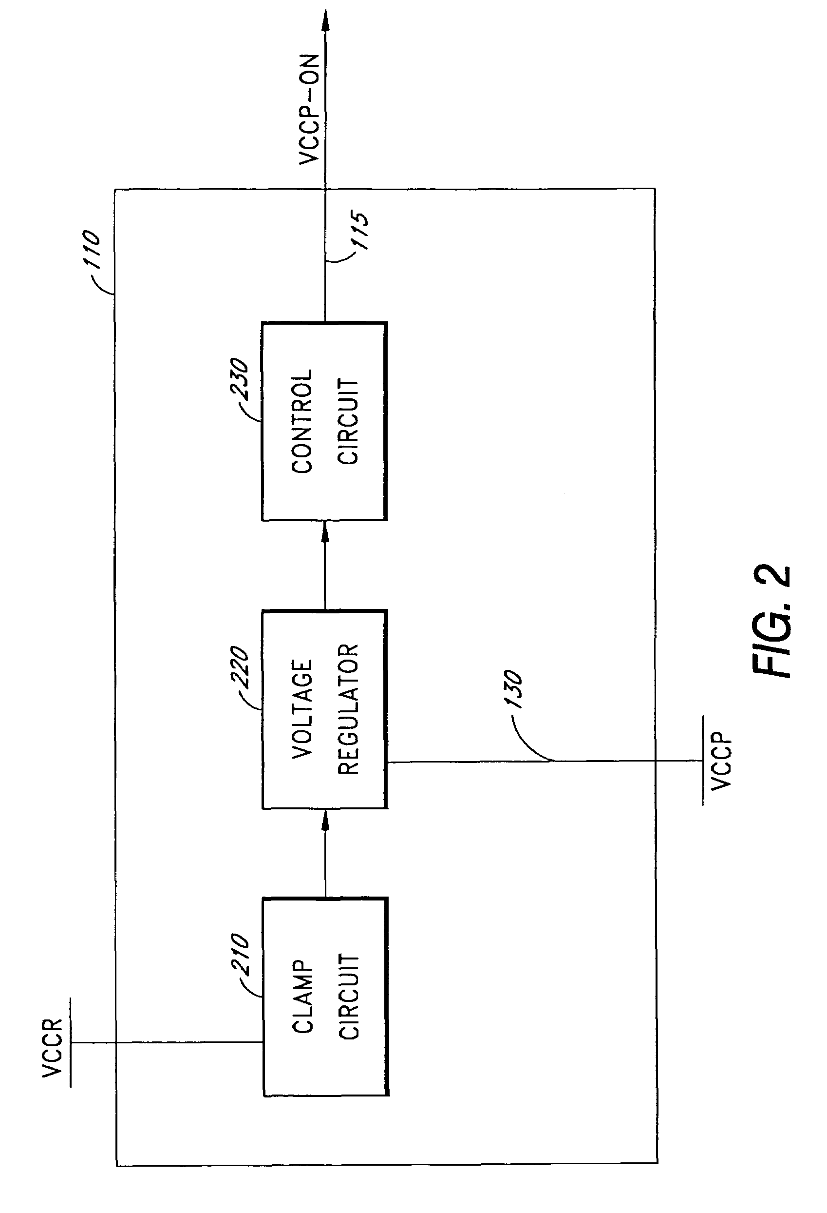
A voltage control circuit provides a test supply voltage during manufacturing and testing of a semiconductor device and provides an operational supply voltage after certification of the semiconductor device. The operational supply voltage is lower than the test supply voltage. The voltage control circuit includes a clamp circuit having a plurality of voltage regulation devices, typically diodes. The voltage regulation devices control an output of the clamp circuit. A voltage regulator is electrically coupled to the clamp circuit and generates a first control signal based upon the output of the clamp circuit. A charge pump then receives the control signal from the voltage regulator, and, based on the value of the control signal, the charge pump generates the test supply voltage. At least one bypass device is connected to at least one of the plurality of voltage regulation devices. The bypass device is activated following the certification of the semiconductor device. Once activated, the bypass device bypasses the respective voltage regulation device from the clamp circuit, which limits the output of the clamp circuit. The voltage regulator then generates a second control signal based upon the limited output of the clamp circuit. The second control signal is provided to the charge pump to generate the operational supply voltage.

Description

RELATED APPLICATIONS[0001]The present application is a continuation of U.S. patent application Ser. No. 09 / 387,263 filed on Aug. 31, 1999, now U.S. Pat. No. 6,351,180 the contents of which are incorporated herein by reference.BACKGROUND OF THE INVENTION[0002]1. Field of the Invention[0003]The present invention relates generally to semiconductor integrated circuits. More specifically, the present invention relates to differential voltage regulators used in semiconductor devices[0004]2. Description of the Related Art[0005]A semiconductor device may be designed for any of a wide variety of applications. Typically, the device includes logic circuitry to receive, manipulate or store input data. The circuitry subsequently generates the same or modified data at an output terminal of the device. Depending on the type of semiconductor device or the circuit in which it is used, the device typically includes circuits which provide internal power signals that are regulated to be substantially i...

Claims


Application Information

Patent Timeline
Patent Type & Authority Patents(United States)
IPC IPC(8): G05F1/10G05F3/02G11C5/14G11C29/12
CPCG11C5/145G11C29/12G11C29/12005
Inventor SHER, JOSEPH C.LOUGHMILLER, DANIEL R.
Owner MICRON TECH INC
Learn More