Image pickup apparatus and fingerprint recognition apparatus
a fingerprint recognition and image pickup technology, applied in image data processing, instruments, television systems, etc., can solve the problems of increasing costs and lengthening processing tim
- Summary
- Abstract
- Description
- Claims
- Application Information
AI Technical Summary
Benefits of technology
Problems solved by technology
Method used
Image
Examples
first embodiment
[0028]FIG. 4A is a perspective view of a fingerprint image input device of a fingerprint recognition apparatus of the present invention. FIG. 4B is a plan view of a structure of the fingerprint image input device of the fingerprint recognition apparatus of the present invention and shows a shading tendency of a sensor signal in the case in which the present invention is not applied.
[0029]As shown in FIG. 4B, one LED 202 for illumination is arranged in the vicinity of a center on each side in a vertical scanning direction of a solid-state image pickup element 201, such as a CMOS sensor, of a fingerprint image input device 200. A finger 100 is placed on the solid-state image pickup element 201, and light is irradiated on the finger 100 from the LEDs 202. The irradiated light is transmitted through or scattered in the inside of the finger to be incident on the solid-state image pickup element 201 side.
[0030]Then, the solid-state image pickup element 201 aligns a longitudinal direction ...
second embodiment
[0044]In the first embodiment, shading correction is performed by changing an opening shape of a pixel portion. In this embodiment, shading correction is performed by controlling drive timing within a scanning time for one frame.
[0045]Here, control of storage time of a pixel portion is performed by an electronic shutter (rolling shutter).
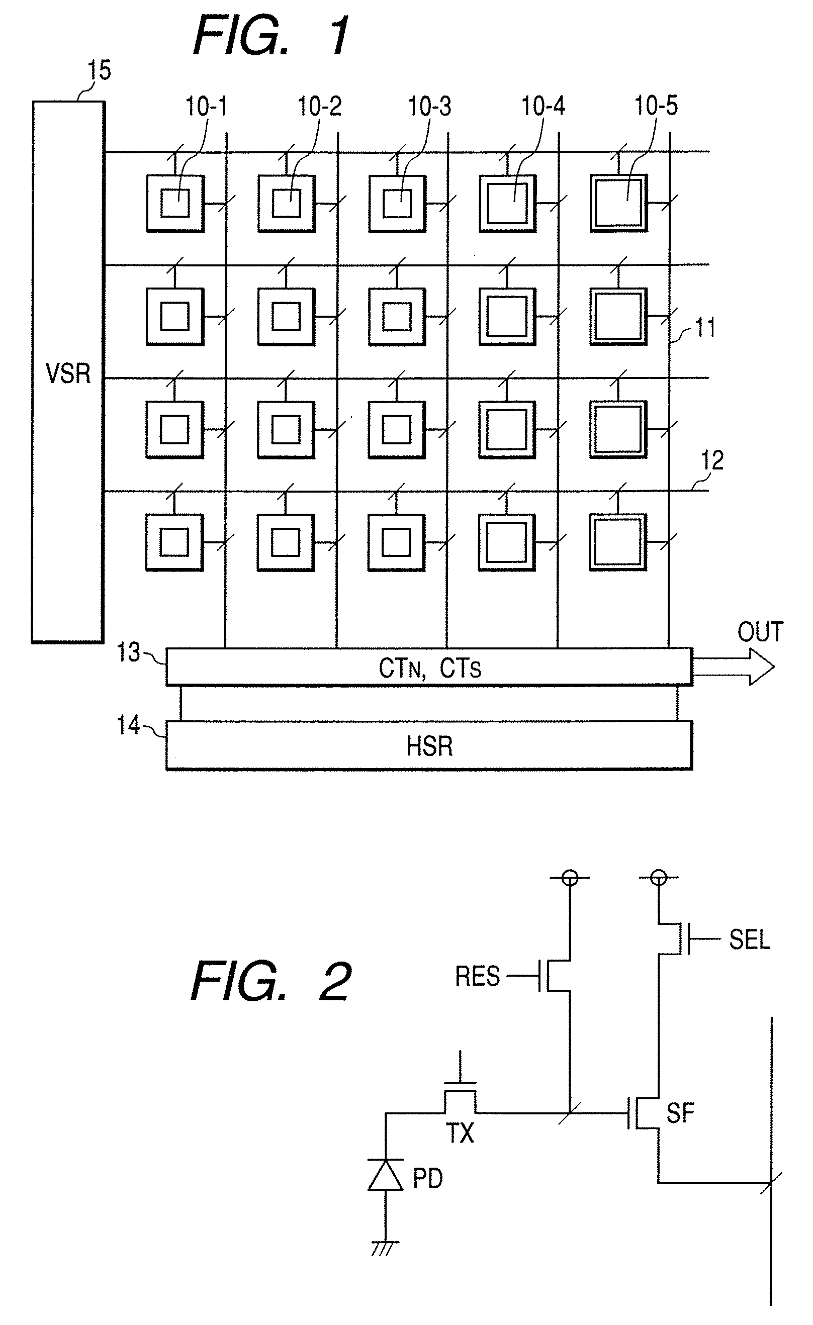
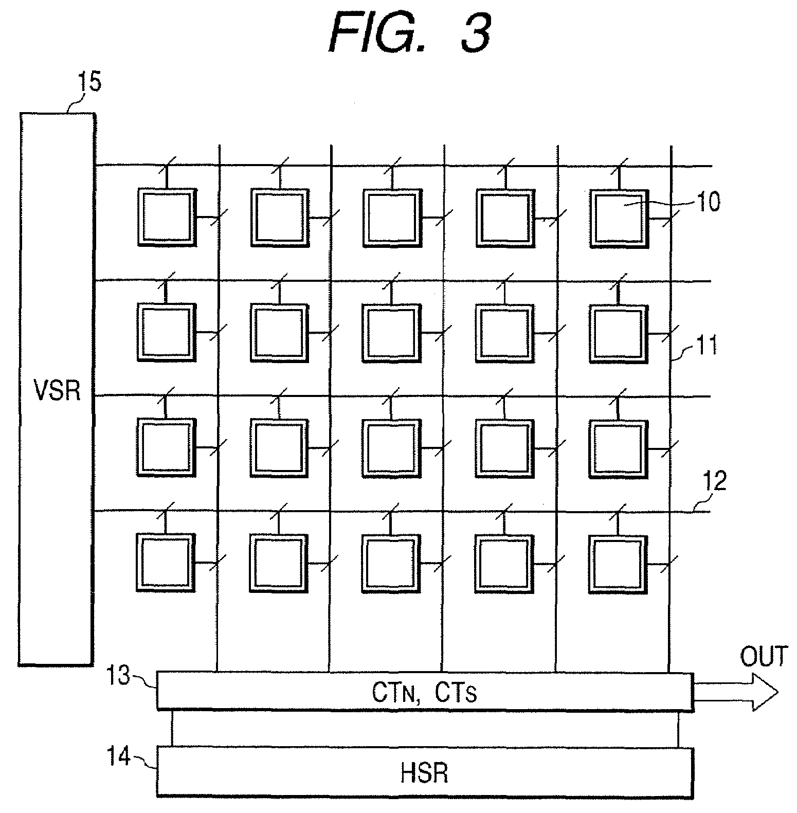
[0046]FIG. 6 is a diagram schematically showing a solid-state image pickup element used in this embodiment. One pixel of the pixel portion has the same pixel structure as that shown in FIG. 2. In addition, opening shapes of pixels of a pixel area 20 are uniform for all pixels.
[0047]In FIG. 6, reference numeral 20 denotes a pixel area constituted by arranging a plurality of pixels; 21, a first vertical scanning circuit (Vs·SR) such as a shift register for sequentially selecting pixel rows to be read; 22, a second vertical scanning circuit (Vc·SR) such as a shift register for sequentially resetting pixel rows in order to start storage; 23, an entire p...
PUM
 Abstract
Description
Claims
Application Information


