Infrared detector
a detector and infrared technology, applied in the field of infrared detectors, can solve the problems of difficult use of algaas layer as the layer in which quantum dots are embedded, and achieve the effect of reducing dark curren
- Summary
- Abstract
- Description
- Claims
- Application Information
AI Technical Summary
Benefits of technology
Problems solved by technology
Method used
Image
Examples
first embodiment
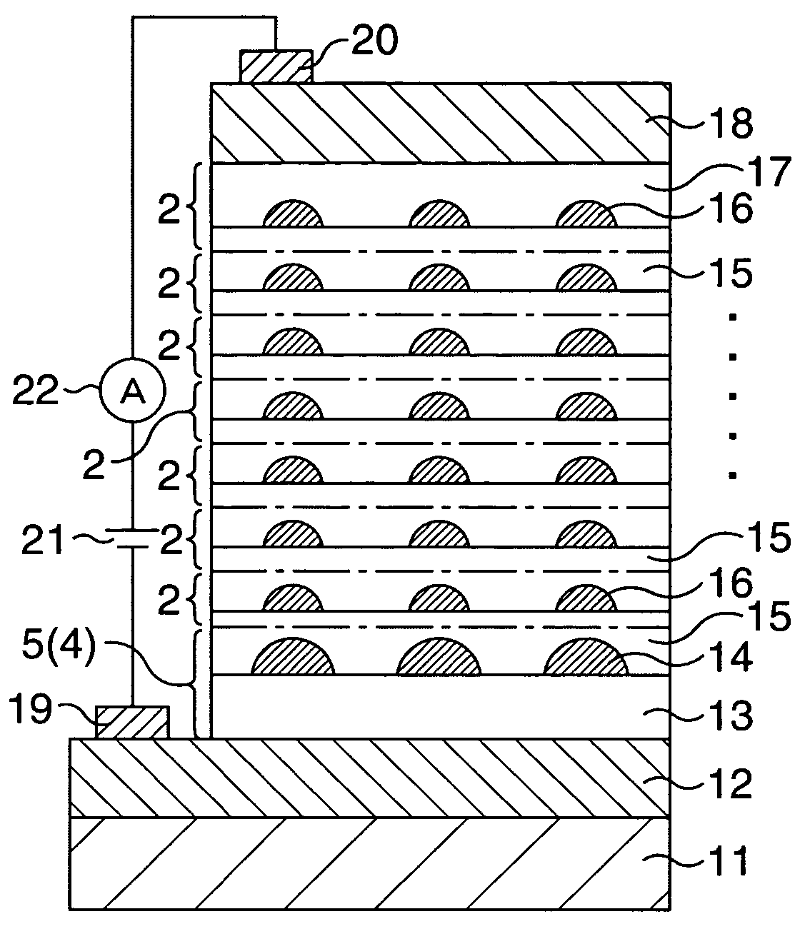
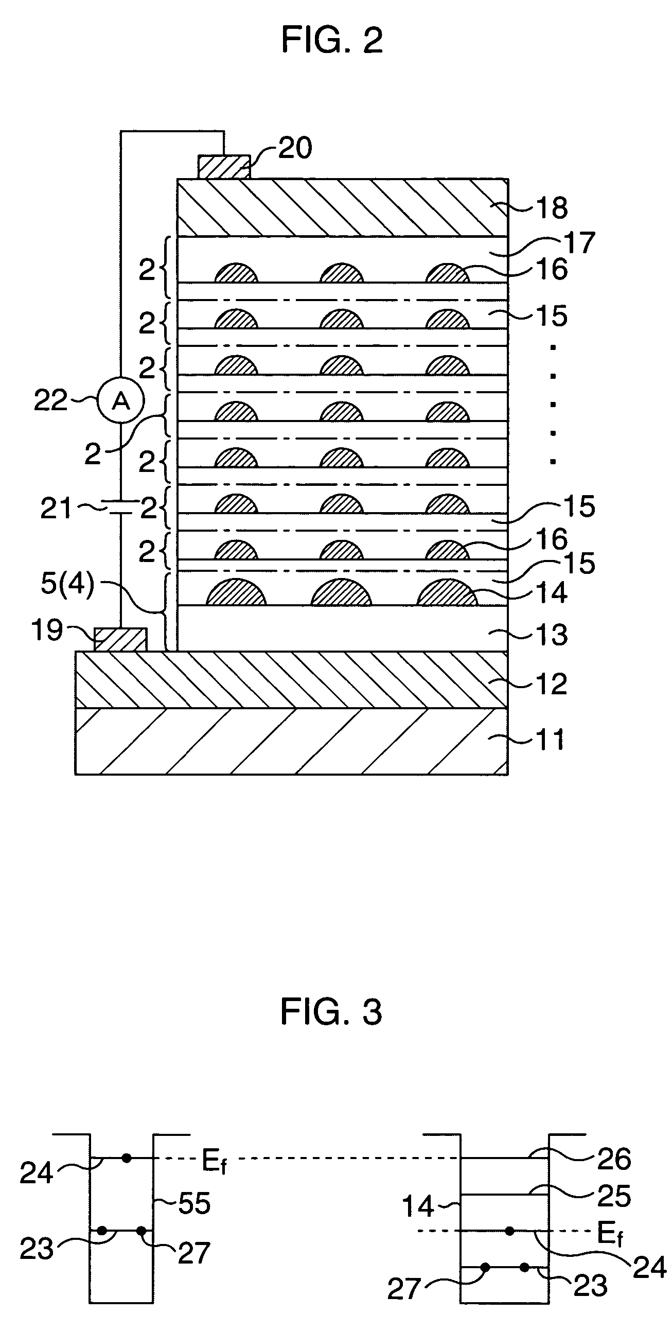
[0053]First, a first embodiment of the present invention will be described. FIG. 2 is a sectional view showing a conceptual constitution of a QDIP according to the first embodiment of the present invention.
[0054]First, an n-type GaAs layer 12, for example, with a thickness of about 1000 nm (=1 μm) and a Si concentration of about 2×1018 cm−3 is grown as a bottom electrode layer on a semi-insulating GaAs substrate 11 at a substrate temperature of, for example, 600° C. by a molecular beam epitaxial method.
[0055]Then, an i-type GaAs layer 13 with a thickness of, for example, 50 nm is grown on the n-type GaAs layer 12. Incidentally, the substrate temperature is lowered from 600° C. to a temperature suitable for the formation of quantum dots, for example, 500° C. while the i-type GaAs layer 13 is grown.
[0056]Subsequently, while the substrate temperature is maintained at 500° C., InAs is supplied such that the growth rate becomes, for example, 0.2 ML (monolayer) / s (second). When a certain ...
second embodiment
[0078]Next, a second embodiment of the present invention will be described. FIG. 6 is a sectional view showing a conceptual constitution of a QDIP according to the second embodiment of the present invention.
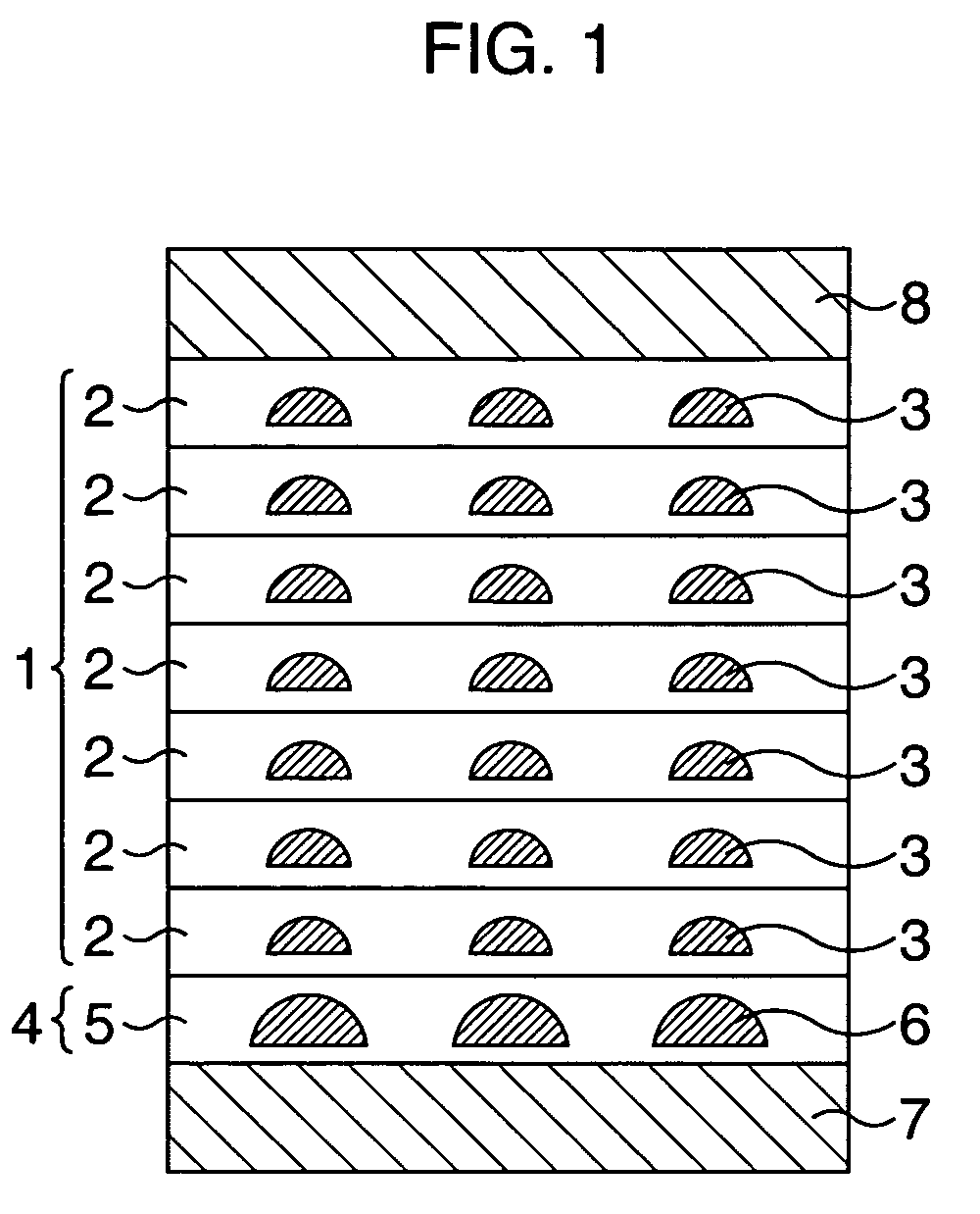
[0079]In the second embodiment, after the large quantum dots 14 are grown on the i-type GaAs layer 13 with the total supply amount of InAs set to 2.5 ML and the i-type GaAs layer 15 covering the quantum dots 14 is formed, the formation of other quantum dots 14 and the formation of another i-type GaAs layer 15 are repeated twice. As a result, the number of the quantum dot layers 5, that is, the dark current reducing layers 4 each including the large quantum dots 14 are three. The other constitution is the same as that of the first embodiment.
[0080]In such a second embodiment, rises of conduction-band edges of the quantum dots in the second and third dark current reducing layers 4 are added to a rise in the first layer. Therefore, the barrier to electrons becomes higher and the dar...
third embodiment
[0081]Next, a third embodiment of the present invention will be described. FIG. 7 is a sectional view showing a conceptual constitution of a QDIP according to the third embodiment of the present invention.
[0082]First, an n-type GaAs layer 12, for example, with a thickness of about 1000 nm (=1 μm) and a Si concentration of about 2×1018 cm−3 is grown as a bottom electrode layer on a semi-insulating GaAs substrate 11 at a substrate temperature of, for example, 600° C. by a molecular beam epitaxial method.
[0083]Then, an i-type GaAs layer 13 with a thickness of, for example, 50 nm is grown on the n-type GaAs layer 12. Incidentally, the substrate temperature is lowered from 600° C. to a temperature lower than in the first embodiment, for example, 480° C. while the i-type GaAs layer 13 is grown.
[0084]Subsequently, while the substrate temperature is maintained at 480° C., InAs is supplied such that the growth rate becomes, for example, 0.2 ML (monolayer) / s (second). In the present embodimen...
PUM
 Abstract
Description
Claims
Application Information


