Buried short location determination using voltage contrast inspection

a voltage contrast and location determination technology, applied in the field of semiconductor fabrication, can solve the problems of inability to locate buried shorts, inability to apply area accelerated vc inspection to these structures, and high cost and time-consuming

Inactive Publication Date: 2009-01-06
GLOBALFOUNDRIES INC
View PDF7 Cites 105 Cited by
  • Summary
  • Abstract
  • Description
  • Claims
  • Application Information

AI Technical Summary

Problems solved by technology

Unfortunately, in some cases a defect is not visible.
The location cannot, however, be established for buried shorts because the illumination brightness of the tine containing the short will be the same regardless of the short's location.
Unfortunately, area accelerated VC inspection cannot be applied to these structures.
Unfortunately, this approach is expensive and time consuming and results in wafer scrap.

Method used


Image

  • Buried short location determination using voltage contrast inspection
  • Buried short location determination using voltage contrast inspection
  • Buried short location determination using voltage contrast inspection

Examples


Embodiment Construction

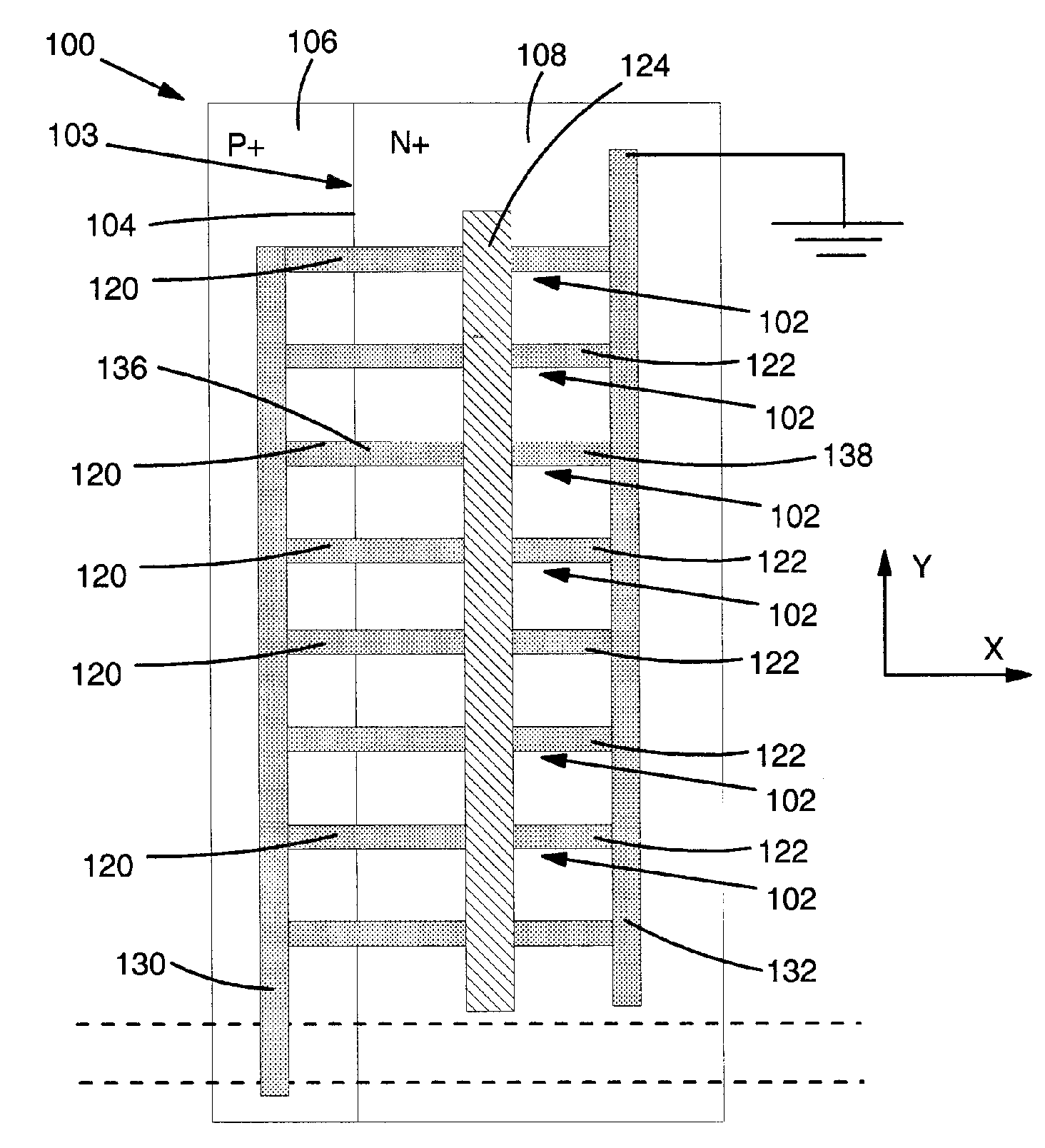
[0026]Turning to the drawings, FIGS. 5A-C show various embodiments of a test structure 100 for determining a location of a buried short using voltage contrast (VC) inspection according to the invention. “Buried short” as used herein includes any manner of short that is not visible through non-invasive, simple physical inspection. As such, a buried short may not be literally buried, but may be smaller than is visible through non-invasive, simple physical inspection. A buried short 140 (FIG. 7) may include, for example, a short such as a silicide pipe, a gate oxide (e.g., silicon dioxide) short, a buried metal short, a buried substrate to active region short, or any other type of short. Test structure 100 may include a plurality of test elements 102 each having a structure 103 allowing current flow in only one direction and only when forward biased. A location of a buried short 140 (FIG. 7) within test structure 100 can be determined using structure 103 using VC inspection, as will be...


PUM


Abstract

Structure and methods of determining the complete location of a buried short using voltage contrast inspection are disclosed. In one embodiment, a method includes providing a test structure having a PN junction thereunder; and using the PN junction to determine the location of the buried short using voltage contrast (VC) inspection. A test structure may include a plurality of test elements each having a PN junction thereunder, wherein a location of the buried short within the test structure can be determined using the PN junction and the VC inspection. The PN junction forces a change in illumination brightness of a test element including the buried short, thus allowing determination of the complete location of a buried short.

Description

BACKGROUND OF THE INVENTION[0001]1. Technical Field[0002]The invention relates generally to semiconductor fabrication, and more particularly, to test structures and a method of determining the complete location of a buried short using voltage contrast inspection.[0003]2. Background Art[0004]In-line voltage contrast (VC) inspection is a powerful technique for detecting and isolating yield limiting defects in the semiconductor fabricating industry. In-line VC inspection includes scanning the wafer surface in which test structures exist with a scanning electron microscope (SEM). As the inspection proceeds, the SEM induces charge on all electrically floating elements whereas any grounded elements remain at zero potential. This potential difference is visible to the SEM. In particular, for electron landing energies less than the second crossover of the secondary electron yield curve (approximately 1.5 keV for tungsten (W) and copper (Cu)), grounded elements appear bright whereas floating...

Claims


Application Information

Patent Timeline
Patent Type & Authority Patents(United States)
IPC IPC(8): G01R31/305G01R31/28
CPCG01R31/2632G01R31/311
Inventor PATTERSON, OLIVER D.WILDMAN, HORATIO S.
Owner GLOBALFOUNDRIES INC
Why Eureka
Try Eureka