
Process for finFET spacer formation

a technology of spacers and finfets, applied in the direction of basic electric elements, electrical equipment, semiconductor devices, etc., can solve the problems of difficult to employ current processes for forming finfets

Active Publication Date: 2009-01-13
GLOBALFOUNDRIES US INC
View PDF13 Cites 52 Cited by
  • Summary
  • Abstract
  • Description
  • Claims
  • Application Information

AI Technical Summary

Problems solved by technology

However, given the three dimensional structure of the finFET, current processes for forming the finFET are difficult to employ because the spacer is undesirably formed about the source and the drain regions.

Method used


Image

  • Process for finFET spacer formation
  • Process for finFET spacer formation
  • Process for finFET spacer formation

Examples


Embodiment Construction

[0026]The detailed description explains the preferred embodiments of the invention, together with advantages and features, by way of example with reference to the drawings.

[0027]Disclosed herein are processes for forming the spacer of a finFET structure. It should be noted, however, that the processes described herein for forming the spacer are equally applicable to any fin-based, multigate transistor architecture regardless of number of gates. Moreover, the present invention may be practiced in conjunction with a various integrated circuit techniques that are conventionally used in the art, and only so much of the commonly practiced process steps are included herein as much as necessary to provide an understanding the present invention.

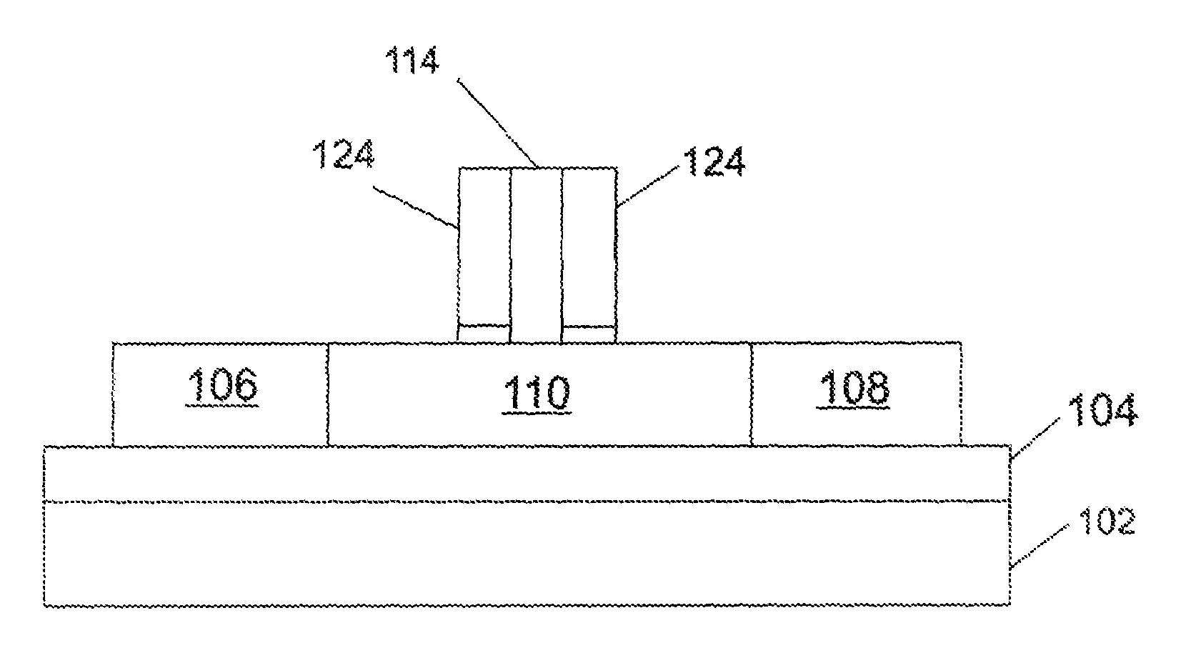
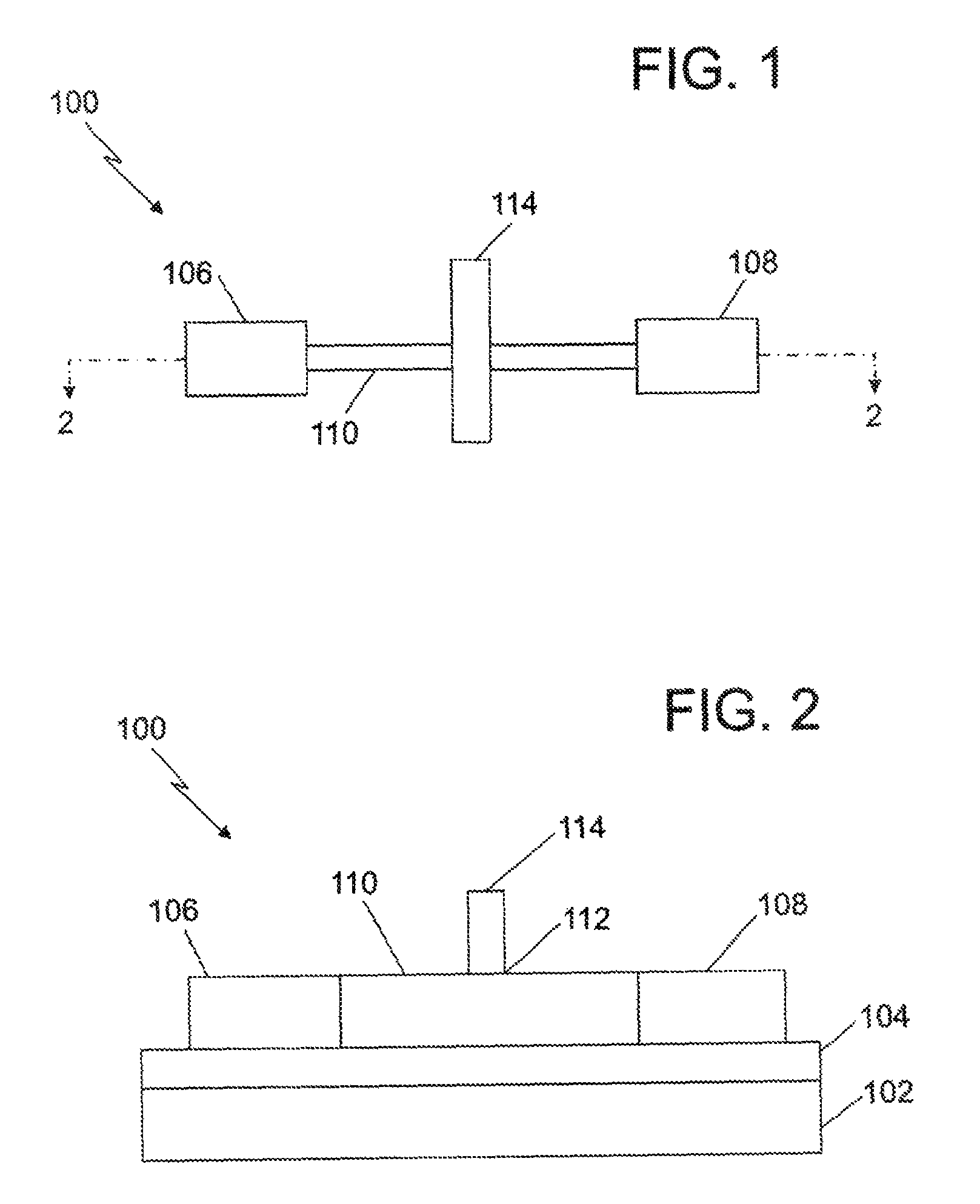
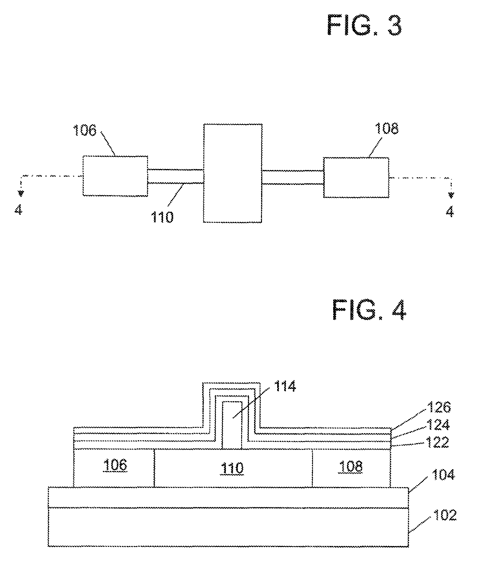
[0028]As shown in FIGS. 1 and 2, the illustrated finFET structure, generally designated by reference numeral 100, is fabricated on a silicon substrate 102 having a buried oxide layer 104 and includes a silicon source island 106 and a drain island 108...


PUM


Abstract

A process for finFET spacer formation generally includes depositing, in order, a conformal liner material, a conformal spacer material, and a conformal capping material onto the finFET structure; tilt implanting dopant ions into portions of the capping layer about the gate structure; selectively removing undoped capping material about the source and drain regions; selectively removing exposed portions of the spacer material; selectively removing exposed portions of the capping material; anisotropically removing a portion of the spacer material so as to expose a top surface of the gate material and isolate the spacer material to sidewalls of the gate structure; and removing the oxide liner from the fin to form the spacer on the finFET structure.

Description

BACKGROUND OF THE INVENTION[0001]1. Field of the Invention[0002]This invention generally relates to finFET spacer formation.[0003]2. Description of the Background[0004]The term FinFET generally refers to a nonplanar, double-gate transistor. Integrated circuits that include FinFETs may be fabricated on a bulk silicon substrate or, more commonly, on a silicon-on-insulator (SOI) wafer that includes an active SOI layer of a single crystal semiconductor, such as silicon, a semiconductor substrate, and a buried insulator layer, e.g., a buried oxide layer that separates and electrically isolates the semiconductor substrate from the SOI layer. Each FinFET generally includes a narrow vertical fin body of single crystal semiconductor material with vertically-projecting sidewalls. A gate contact or electrode intersects a channel region of the fin body and is isolated electrically from the fin body by a thin gate dielectric layer. At opposite ends of the fin body are heavily-doped source / drain ...

Claims


Application Information

Patent Timeline
IPC IPC(8): H01L21/00
CPCH01L29/66795H01L29/785
Inventor CHENG, KANGGUOLI, XIWISE, RICHARD S.
Owner GLOBALFOUNDRIES US INC
Learn More