Memory device with improved writing capabilities

a memory device and writing capability technology, applied in the field of memory devices, can solve the problems of inefficiency in recovering manufacturing errors, write failure and read failure, instability, etc., and achieve the effects of reducing the vdd supply of the column, reducing the drive of the pmos pull-up of the memory cell, and facilitating the force of access transistors

Active Publication Date: 2009-02-03
INFINEON TECH AG
View PDF5 Cites 23 Cited by
  • Summary
  • Abstract
  • Description
  • Claims
  • Application Information

AI Technical Summary

Benefits of technology

[0010]Embodiments of the invention are based on the finding that the reliability of a write operation can be increased when reducing the potential of the bit line below the first potential, e.g. below VSS, when writing the first information value represented by the first potential to the memory element. According to the invention, the bit line is boosted under the first potential during the write operation for at least a time interval so that statistical positive voltage variations increasing the potential to be transferred are at least partly compensated so that the cell has time to flip completely. Therefore, even low voltage technologies may be employed for operating the memory cells.
[0020]According to the invention, the potential controller is also coupled to the further bit line so that either the first or the second information value may differentially be transferred to the memory element during a writing operation. More specifically, the potential controller may be configured to apply the second potential to the bit line (e.g. VDD) and to apply the third potential to the further bit line when writing the second information value to the memory element. Thus, the difference between the potential of the bit line and the potential of the further bit line is increased when compared to the conventional accessing methods by the amount of the third potential undershooting the first potential. Alternatively, the potential controller may apply the third potential to the bit line and the second potential to the further bit line in order to store the first information value in the memory element.
[0022]The inventive concept may also be applied when writing the second information value to the memory element. More specifically, one embodiment of the invention provides a memory device comprising a memory element for storing the first or the second information value, a bit line coupled to the memory element and a potential controller coupled to the bit line, the potential controller being configured to apply a third potential to the bit line when writing the second information value represented by the second potential to the memory element, the third potential exceeding the second potential. In other words, the potential controller may be configured to increase the potential of the bit line above the second potential in order to mitigate the influence of e.g. negative voltage variations across e.g. an access transistor to increase the potential transmitted through the access transistor.
[0025]In order to improve the write operation, e.g. a wordline boosting can be used which, however, may degrade the stability of the selected cells. The inventive bit line boosting does not negatively affect the stability of the memory cell.
[0027]Another solution is to decrease the VDD supply of the column to which the cell to be written pertains. The cells which are not accessed to are not influenced by this change. The benefit is that the drive of the PMOS pull-up of the memory cell is decreased and therefore the access transistor can more easily force a “0”. However, the drive of e.g. a PMOS driving the complementary node of the bit cell is also decreased and consequently establishing VDD on this node is made more difficult. Moreover, one VDD vertical track per memory cell column has to be built in the layout which increases an area demand which e.g. make more difficult a robust VDD power net.
[0028]An aspect of the present invention is to boost a write potential below VSS on the bit line that forces the “0” into the bitcell. Since the bit line is the source of the access transistor, this increases significantly the drive current of that transistor so that the pull-up can efficiently be mitigated. This is an effective approach since the access transistor is by far (3 times) the most sensitive transistor of the bitcell with respect to the write operation.

Problems solved by technology

When manufacturing SRAM cells in deep sub-micron technologies characteristics, errors like instability, write fail and read fail are expected due to large statistical deviations of the SRAM cells.
Since a recovery of the manufacturing errors is costly, designing memory peripheries only addressing the bit cells is not efficient.
For example, due to a high sensitivity of memory cells with respect to statistical fluctuations of parameters of elements forming the memory cells, e.g. transistors, the write operation of e.g. SRAM cells limits the possibility of employing a low voltage technology (using e.g. VDD=0.75 V) for memory cells.
If the resulting potential at the memory cell exceeds a certain threshold determined by the low voltage technology (e.g. 0.35 V), then a write error occurs.
For example, if the threshold voltage of the access transistor is sufficiently high, this can lead to the impossibility of writing the “0” into the cell.

Method used


Image

  • Memory device with improved writing capabilities
  • Memory device with improved writing capabilities
  • Memory device with improved writing capabilities

Examples


Embodiment Construction

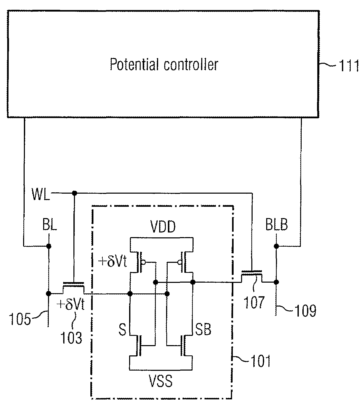
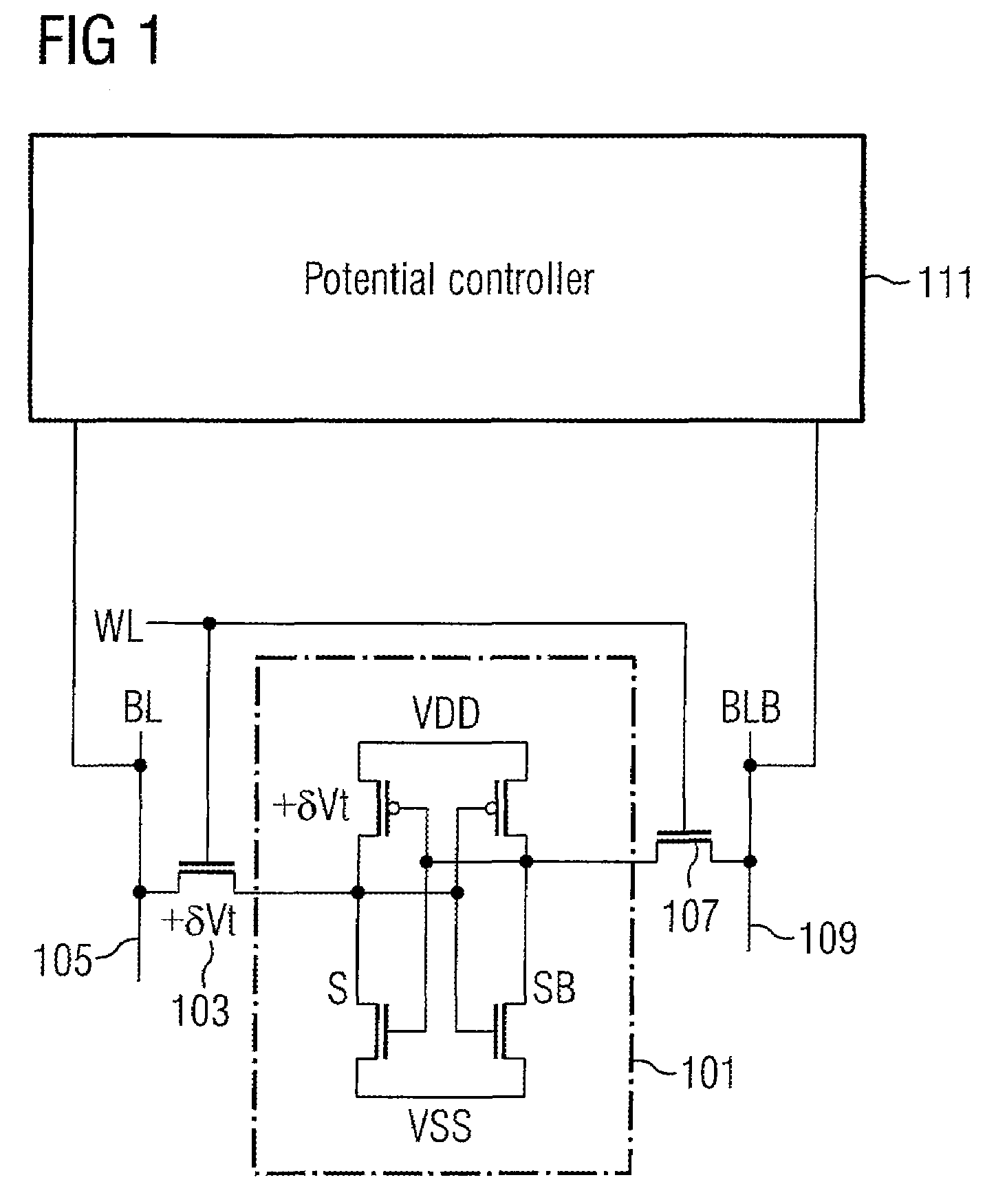
[0038]The memory device shown in FIG. 1 comprises a memory element 101 coupled via a transistor 103 to a bit line 105. The memory element 101 is further coupled by a further switch 107 to a further bit line 109.

[0039]The switches 103 and 107 are formed by transistors having control gates coupled to a wordline WL. The memory device further comprises a potential controller 111 having a first terminal coupled to the bit line 105 (BL) and a second terminal coupled to the further bit line 109 (BLB).

[0040]As depicted in FIG. 1, across the transistor 103 a threshold voltage variation +δVt may be present, which may increase the absolute threshold voltage Vt when writing a “0” from the bit line 105 to the memory cell by e.g. a weak N access device. Correspondingly, the varying voltage across the transistor 103 may contribute to a reduction of the absolute voltage Vt when e.g. writing a “0” via the bit line 105 for the case of a strong P load.

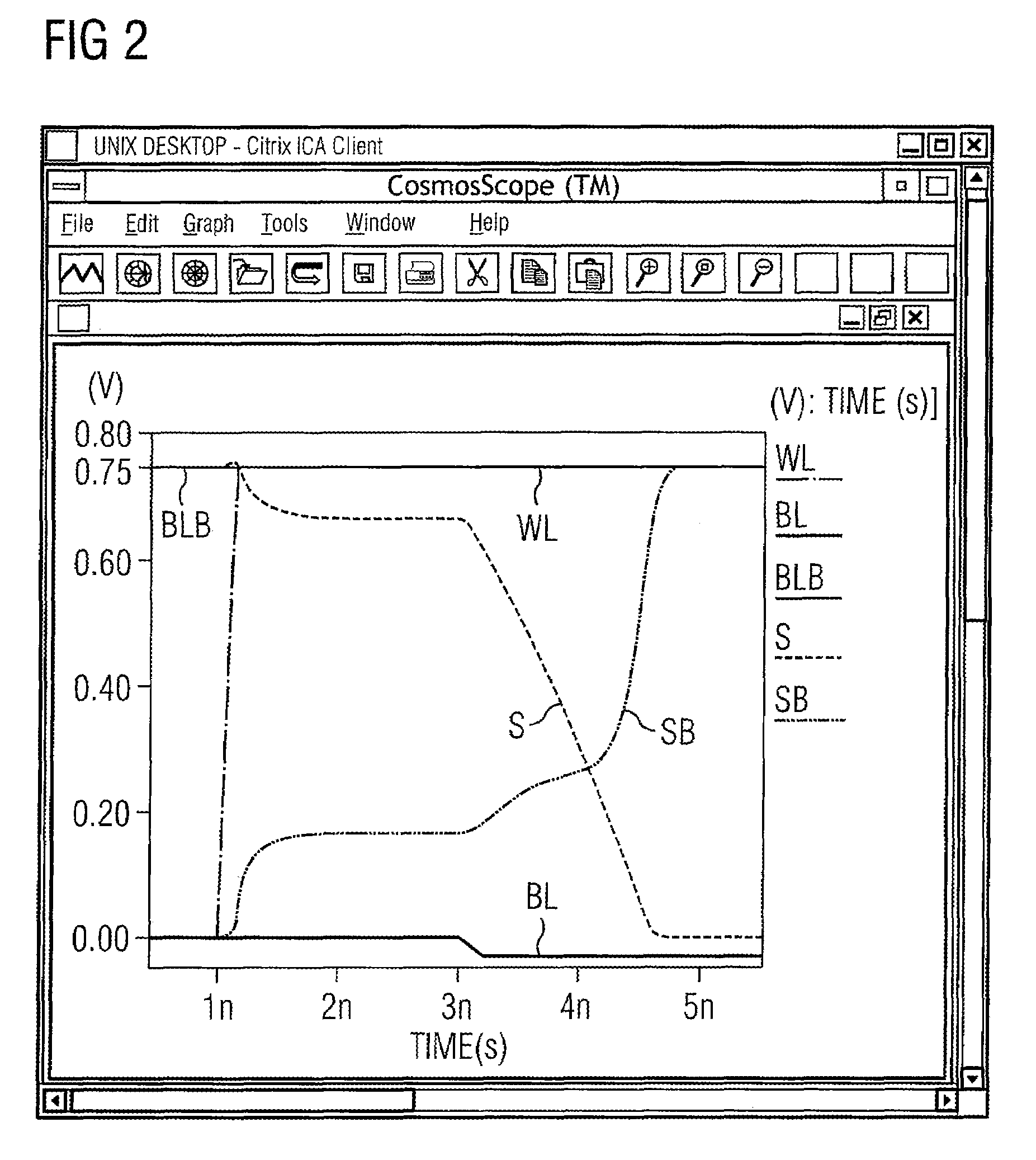
[0041]The memory element 101 is accessed to via th...


PUM


Abstract

Method and memory device for reliably writing an information value to a memory element of the memory device. A first information value is represented by a first potential and a second information value is represented by a second potential. A bit line is provided for writing either the first information value or the second information value to the memory element. A potential controller is coupled to the bit line, where the potential controller is configured to apply a third potential to the bit line, which is less than the first potential when writing the first information value to the memory element.

Description

CROSS-REFERENCE TO RELATED APPLICATIONS[0001]This application claims foreign priority benefits under 35 U.S.C. §119 to co-pending European patent application number EP 05 023 410.3, filed 26 Oct. 2005. This related patent application is herein incorporated by reference in its entirety.BACKGROUND OF THE INVENTION[0002]1. Field of the Invention[0003]The invention relates to memory devices.[0004]2. Description of the Related Art[0005]When manufacturing SRAM cells in deep sub-micron technologies characteristics, errors like instability, write fail and read fail are expected due to large statistical deviations of the SRAM cells. Since a recovery of the manufacturing errors is costly, designing memory peripheries only addressing the bit cells is not efficient. The memory periphery has to take the statistical deviations into account.[0006]For example, due to a high sensitivity of memory cells with respect to statistical fluctuations of parameters of elements forming the memory cells, e.g. ...

Claims


Application Information

Patent Timeline
Patent Type & Authority Patents(United States)
IPC IPC(8): G11C11/00
CPCG11C11/419G11C11/413G11C11/34
Inventor GOUIN, VINCENTCHANUSSOT, CHRISTOPHE
Owner INFINEON TECH AG
Why Eureka
Try Eureka