Testing high frequency signals on a trace

a high frequency signal and trace technology, applied in the field of signal monitoring, can solve the problems of increasing the difficulty of effectively testing and measuring signals and components within the circuit, the difficulty for an engineer to locate a failure in the integrated circuit, and the difficulty of effectively tapping and monitoring these internal ic signals, so as to reduce the amount of distortion

Inactive Publication Date: 2009-02-10
AVAGO TECH WIRELESS IP SINGAPORE PTE
View PDF4 Cites 4 Cited by
  • Summary
  • Abstract
  • Description
  • Claims
  • Application Information

AI Technical Summary

Benefits of technology

[0011]The present invention provides a system, apparatus and method for measuring and testing high frequency signals on a trace. In one embodiment of the invention, a footprint is manufactured on a trace to allow the testing of a signal while reducing the amount of distortion caused by prior art structures and methods. In one embodiment, the footprint allows surface mount resistors to be connected to define a particular path for the signal. A first path is provided in which the signal is communicated on the trace between IC components, such as a driver and a receiver. A second path is provided in which the signal is communicated from the trace to a testing or measurement device, such as an oscilloscope.
[0012]In one embodiment of the invention, the footprint is manufactured by partially overlaying a first surface mount area with a second surface mount area. The first and second surface mount areas may be positioned at a 90 degree angle from each other. This footprint design minimizes stub effects and capacitance generated by prior art testing connections.

Problems solved by technology

As integrated circuits have become smaller and signal frequencies within the circuits have increased, the ability to effectively test and measure signals and components within the circuits has become more difficult.
For example, it may be difficult for an engineer to locate a failure in an integrated circuit because of the problems in tapping or extracting an electrical signal internal to the integrated circuit.
The ever-increasing signal frequencies on IC traces have made it difficult to effectively tap and monitor these internal IC signals.
Electromagnetic interferences, including signal reflection and distortion, oftentimes render a tapped signal unusable for monitoring purposes.
Furthermore, footprints on a trace that are designed to allow testing of a signal may reduce the performance of the trace by effectively creating a stub on the trace and / or adding unwanted capacitance.
If sufficiently high frequency signals are being monitored, this dispersion and reflection on the signal may render an oscilloscope reading of the signal to be imprecise or unusable.
This method reduces the reflections but still adds stub and extra capacitance that are caused by the surface mount footprint on the trace.
This stub and capacitance may lead to inaccurate results and distort the signal received by the receiver 204.
At specified frequency of operation, which tends to be more than 1 Gbps, the accuracy of the observed results greatly affects the troubleshooting procedure.
The extra trace on board in mentioned operating conditions adds to the inaccuracy.

Method used


Image

  • Testing high frequency signals on a trace
  • Testing high frequency signals on a trace
  • Testing high frequency signals on a trace

Examples


Embodiment Construction

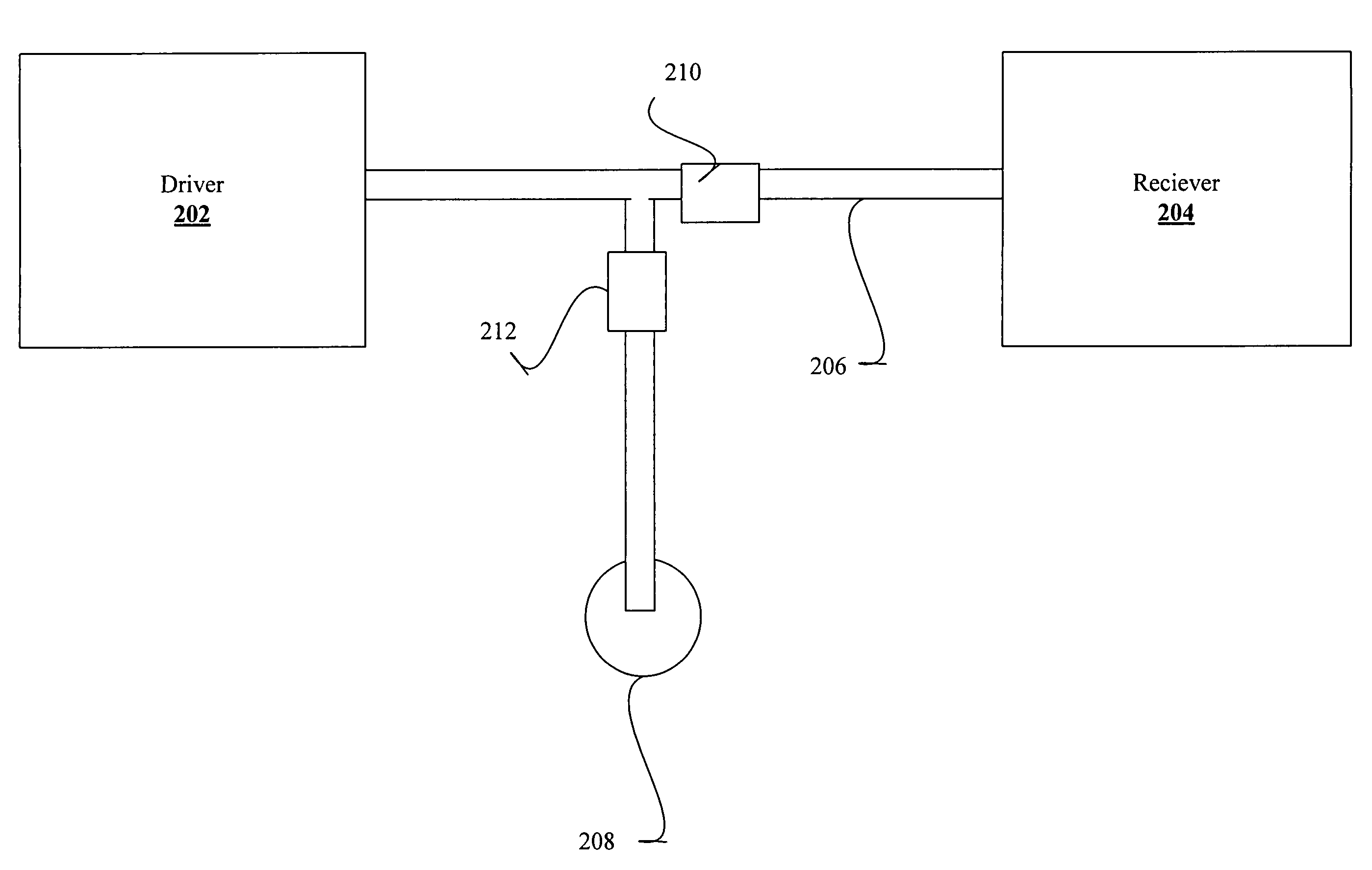
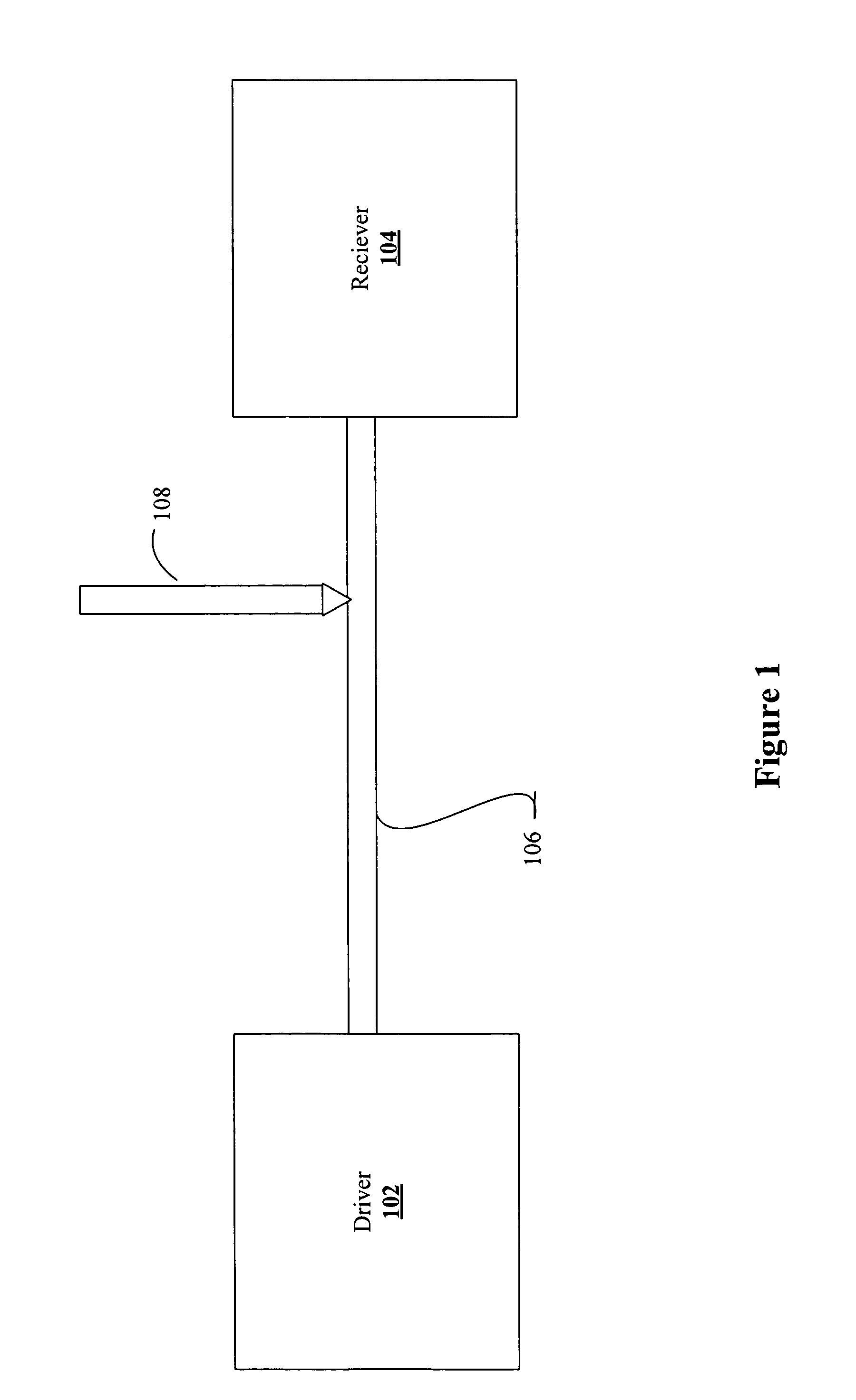
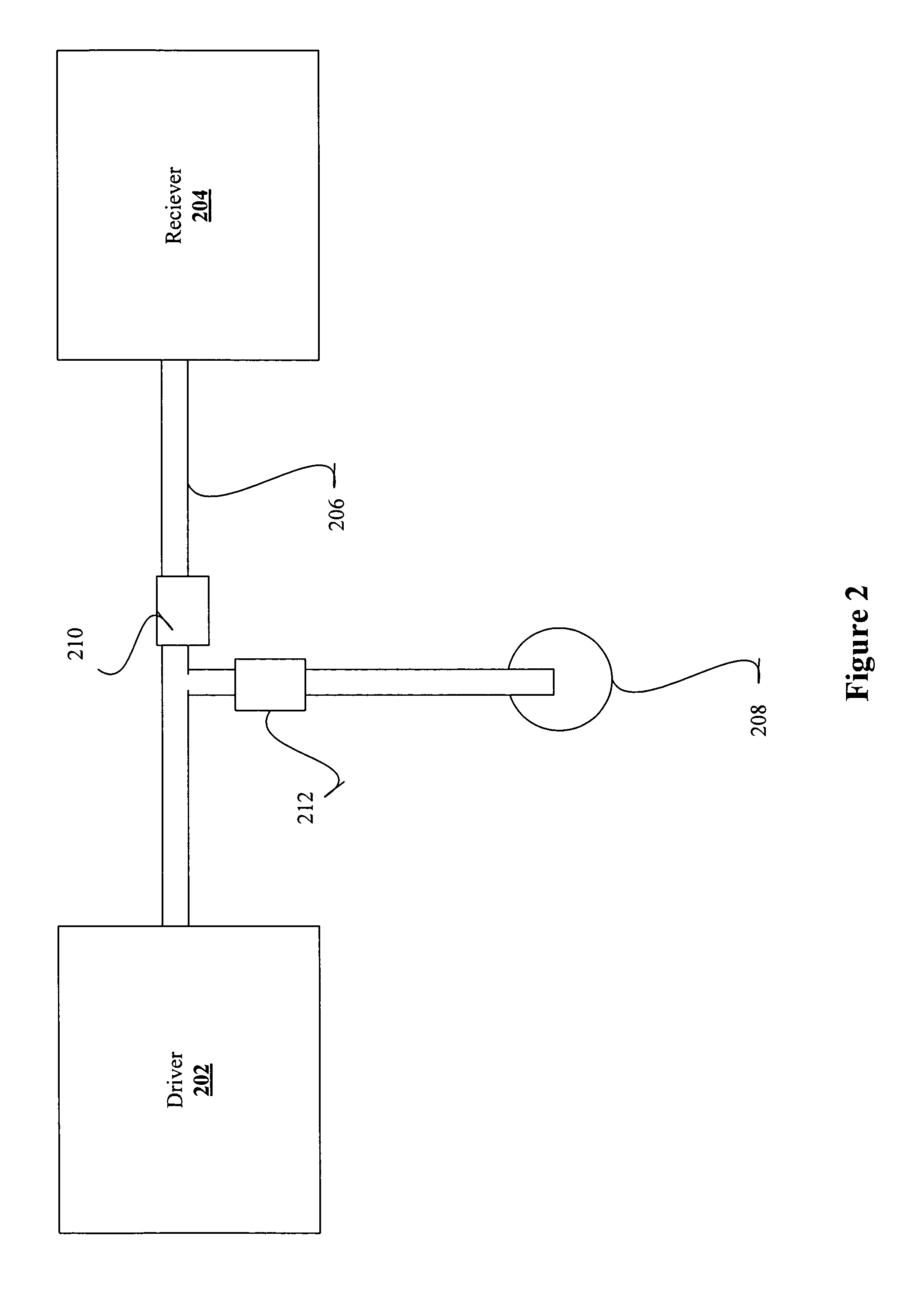
[0021]A system, apparatus and method for observing a high frequency signal on a trace is described. The system may operate in multiple modes including a first mode in which a signal is communicated between a driver and a host, and a second mode in which the signal is communicated to a measurement device, such as an oscilloscope. A footprint that is located on a trace allows for the switching between modes while minimizing the amount of distortion on the signal during either of the modes of operation.

[0022]The invention described herein is explained using specific exemplary details for better understanding. However, the invention disclosed can be worked on by a person skilled in the art without the use of these specific details. The implementations of the invention can be embodied into a multiple types of printed circuit boards. The block diagrams shown are only exemplary implementation as per the rules dictated by the invention. Also, the connections between various components may n...


PUM


Abstract

A system, apparatus and method for testing and measuring high frequency signals on a trace is described. In one embodiment of the invention, a footprint is manufactured on a trace to allow the testing of a signal while reducing the amount of distortion caused by prior art structures and methods. The footprint is designed to reduce stub effects and capacitance on a signal being communicated on the trace.

Description

BACKGROUND[0001]A. Technical Field[0002]This invention relates to signal monitoring, and more particularly, to testing high frequency signals on a trace.[0003]B. Background of the Invention[0004]The importance of integrated circuitry is well known. Technological advancements have led to continual reduction in the size of integrated components and circuitry. The electronic devices employing integrated circuitry have not only seen a reduction in their size but also an improvement in signal processing efficiency. One reason for the improvement of signal processing is the use of higher frequency signals that are able to communicate large amounts of data within an integrated circuit.[0005]As integrated circuits have become smaller and signal frequencies within the circuits have increased, the ability to effectively test and measure signals and components within the circuits has become more difficult. For example, it may be difficult for an engineer to locate a failure in an integrated ci...

Claims


Application Information

Patent Timeline
Patent Type & Authority Patents(United States)
IPC IPC(8): G01R31/26G01R31/28
CPCG01R31/2822G01R31/2886
Inventor TANG, GEORGE
Owner AVAGO TECH WIRELESS IP SINGAPORE PTE
Why Eureka
Try Eureka