Magnetic random access memory and operating method of the same
a random access and memory technology, applied in the field of magnetic random access memory, can solve the problems of insufficient signal level obtained from memory cells, inability to read circuits at the same time, and inability to achieve high-speed read operation
- Summary
- Abstract
- Description
- Claims
- Application Information
AI Technical Summary
Benefits of technology
Problems solved by technology
Method used
Image

Examples
first embodiment
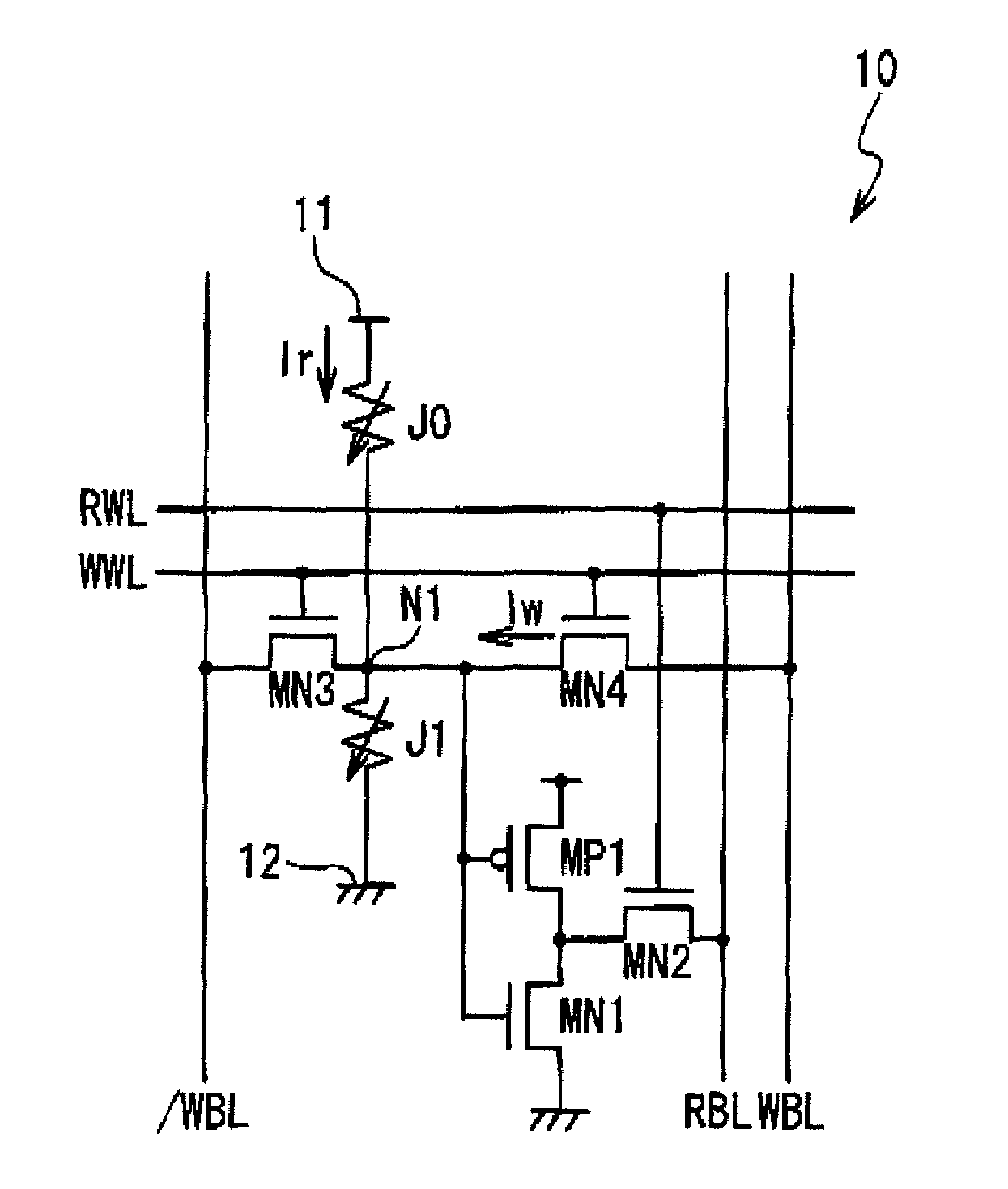
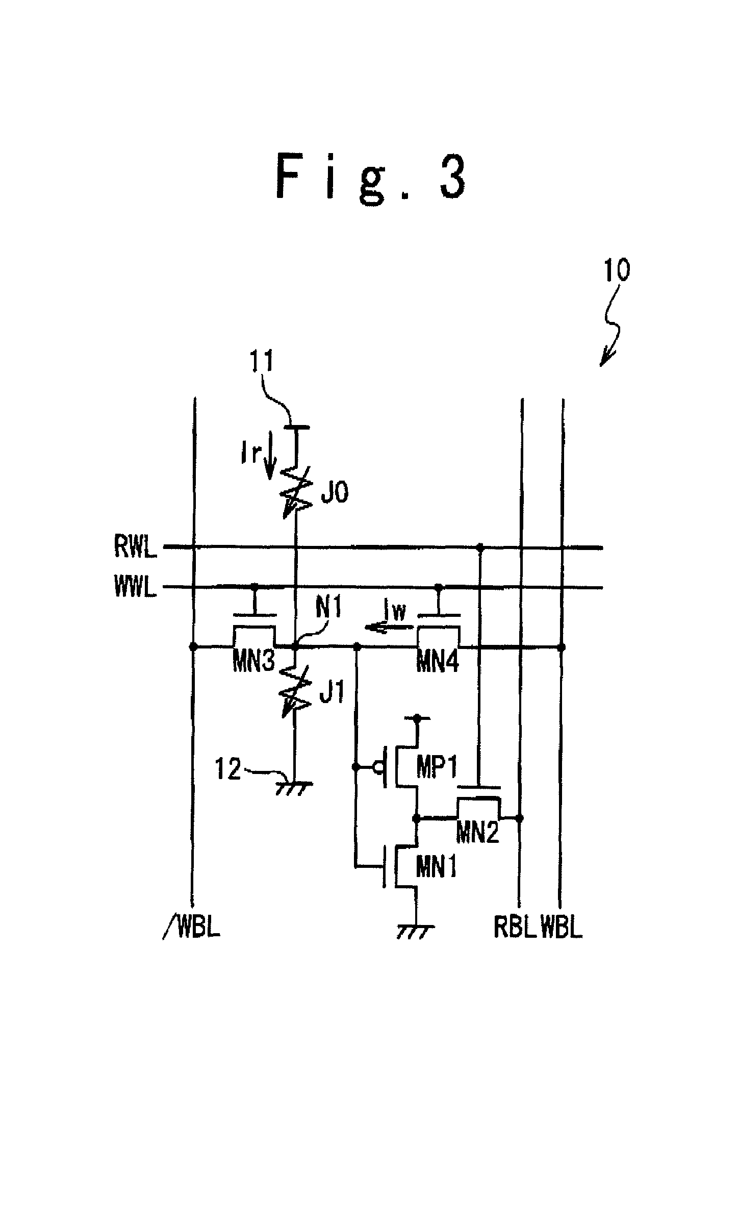
[0062]FIG. 3 is an equivalent circuit diagram illustrating the configuration of a memory cell 10 integrated within an MRAM in a first embodiment. One feature of the MRAM in the first embodiment is that each memory cell 10 incorporates an inverter that amplifies a signal obtained from a series connected magnetoresistive elements.
[0063]Each memory cell 10 is provided with a pair of magnetoresistive elements J0 and J1 each incorporating an MTJ, NMOS transistors MN1 to MN4, and a PMOS transistor MP1. The magnetoresistive element J0 is connected between a power supply terminal 11 and a cell node N1, while the magnetoresistive element J1 is connected between the cell node N1 and a ground terminal 12, The NMOS transistor MN3 is connected between the cell node N1 and a write bitline / WBL, while the NMOS transistor MN4 is connected between the cell node N1 and a write bitline WBL. Gates of the NMOS transistors MN3 and MN4 are connected to the write word line WWL, and the NMOS transistors MN3...
second embodiment
[0083]FIGS. 20 to 23 are diagrams showing the configuration of an MRAM in a second embodiment of the present invention. Differently from the MRAM in the first embodiment, which incorporates an inverter for signal amplification within each memory cell, the MRAM in the second embodiment additionally incorporates sub-sense amplifier circuits 30 each amplifying a signal obtained from the magnetoresistive elements J0 and J1. One sub-sense amplifier circuit 30 is provided for multiple memory cells 20; FIG. 23 shows the configuration in which one sub-sense amplifier circuit 30 is provided for every four memory cells 20. The sub-sense amplifier circuits 30 are arranged in rows and columns in the memory array of in the memory cells 20.
[0084]The memory cells 20 associated with the same sub-sense amplifier circuit 30 are commonly connected to a sub bitline SRBLi. The sub-sense amplifier circuits 30 are designed to output an output signal corresponding to the data stored in the memory cell 20 s...
third embodiment
[0090]FIG. 24 is a block diagram showing the configuration of an MRAM in a third embodiment of the present invention. The MRAM in the third embodiment has a configuration substantially similar to that in the second embodiment. A plurality of memory cells 20A provided in the same column are commonly connected to the same sub sense amplifier circuit 30A, and a plurality of sub sense amplifier circuits 30A provided in the same column are commonly connected to the same sense amplifier circuit 26.
[0091]The difference is that the memory cells 20A and the sub sense amplifier circuits 30A are structured differently from those of the memory cells 20 and the sub sense amplifier circuits 30 of the MRAM in the second embodiment, and that a read word line RWLj is provided for each row of the sub sense amplifier circuits 30A (not for each row of the memory cells 20A) The circuit structure shown in FIG. 18 is used for the sense amplifier circuits 26. It should be noted that inputs SAin of the resp...
PUM
 Abstract
Description
Claims
Application Information
 - R&D Engineer
- R&D Manager
- IP Professional
- Industry Leading Data Capabilities
- Powerful AI technology
- Patent DNA Extraction
Browse by: Latest US Patents, China's latest patents, Technical Efficacy Thesaurus, Application Domain, Technology Topic.
© 2024 PatSnap. All rights reserved.Legal|Privacy policy|Modern Slavery Act Transparency Statement|Sitemap