Semiconductor device having a trenched insulating layer coated with an oxide semiconductor film

a technology of semiconductor film and insulating layer, which is applied in the direction of solid-state devices, transistors, capacitors, etc., can solve the problems of short-channel effect, achieve excellent ohmic contact, reduce the resistance between oxide semiconductor film and source and drain electrode layers, and reduce the size of transistors

Inactive Publication Date: 2014-09-30
SEMICON ENERGY LAB CO LTD
View PDF192 Cites 7 Cited by
  • Summary
  • Abstract
  • Description
  • Claims
  • Application Information

AI Technical Summary

Benefits of technology

[0007]In order to achieve high-speed operation of a transistor, low power consumption of a transistor, high integration, cost reduction, or the like, it is essential to miniaturize a transistor.
[0036]Further, according to one embodiment of the disclosed invention, the size of a transistor can be sufficiently reduced. When the size of the transistor is sufficiently reduced, the area of a semiconductor device is also reduced and thus the number of semiconductor devices manufactured from one substrate is increased. Accordingly, manufacturing cost of per semiconductor device can be reduced. Since the semiconductor device is downsized, a semiconductor device with a size similar to that of the conventional semiconductor device can have improved functions. In other words, the semiconductor device can be highly integrated. Further, effects of high-speed operation, low power consumption, and the like can be obtained because of a reduction in channel length.

Problems solved by technology

In the case where a transistor is miniaturized, a problem of a short-channel effect is caused.

Method used


Image

  • Semiconductor device having a trenched insulating layer coated with an oxide semiconductor film
  • Semiconductor device having a trenched insulating layer coated with an oxide semiconductor film
  • Semiconductor device having a trenched insulating layer coated with an oxide semiconductor film

Examples


embodiment 1

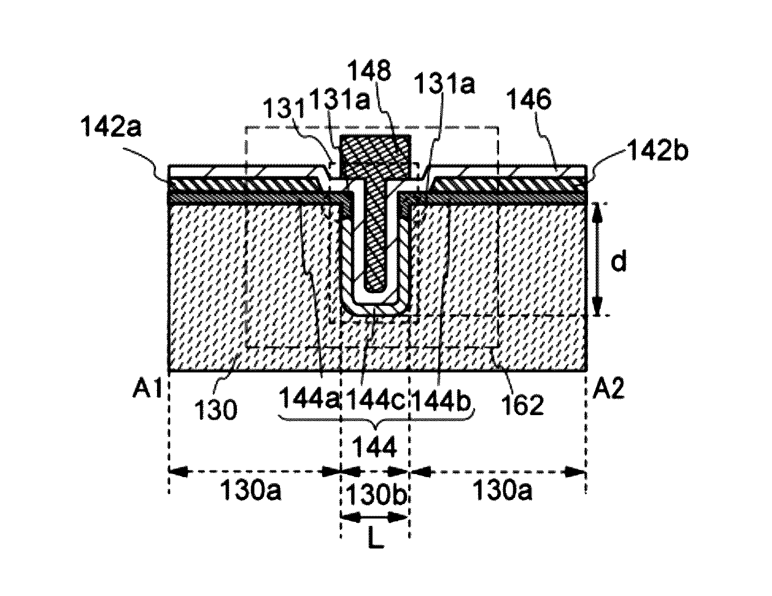
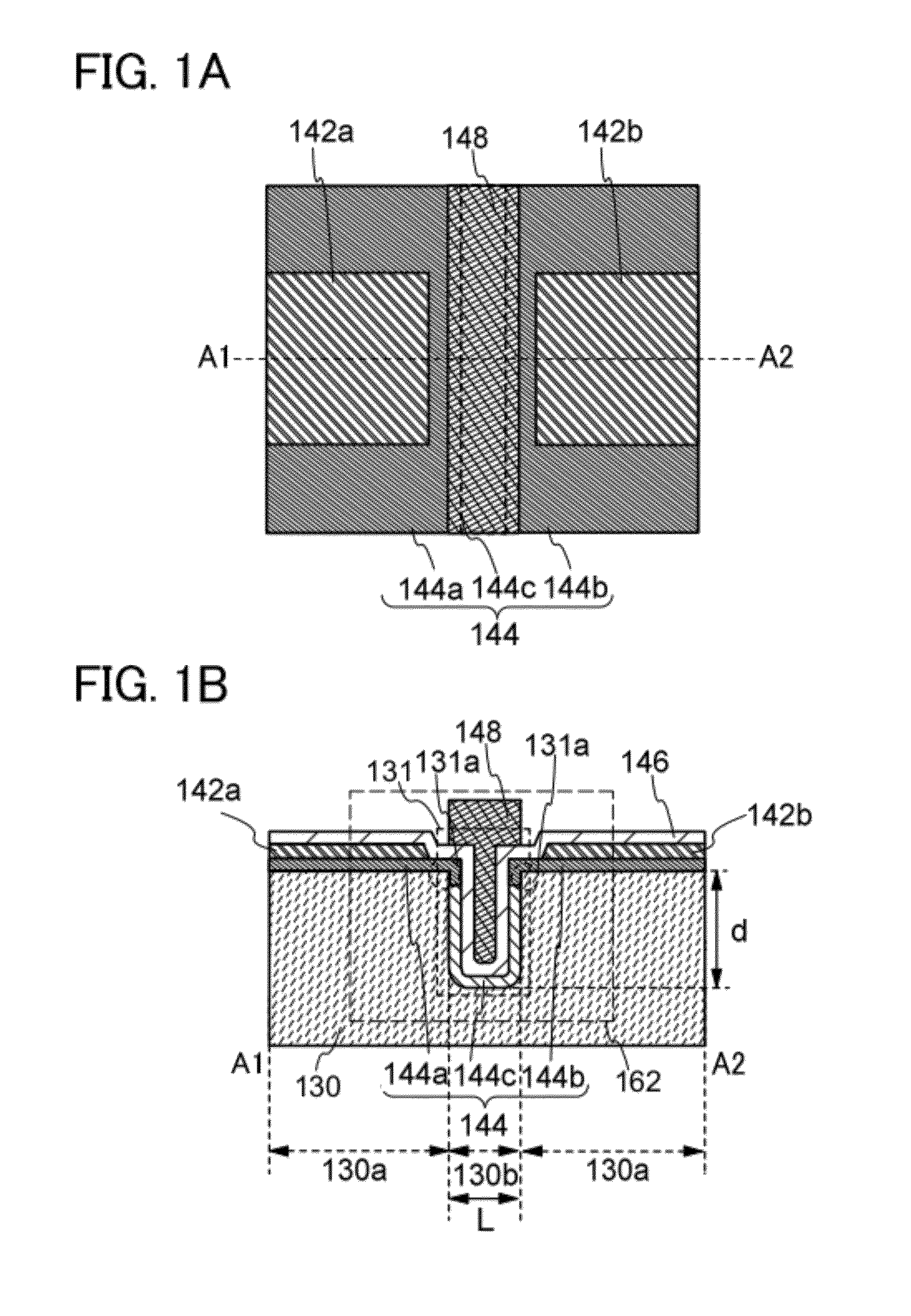
[0064]In this embodiment, an example of a structure of a semiconductor device and a manufacturing process thereof according to one embodiment of the disclosed invention will be described with reference to FIGS. 1A and 1B, FIGS. 2A to 2C, and FIGS. 3A to 3C.

[0065]FIG. 1A illustrates an example of a plan view of a transistor 162 in this embodiment. FIG. 1B illustrates a cross-sectional view taken along chain line A1-A2 in FIG. 1A.

[0066]The transistor 162 described in this embodiment includes an insulating layer 130 provided with a trench 131; an oxide semiconductor film 144 including a source region 144a, a drain region 144b, and a channel formation region 144c; a source electrode layer 142a and a drain electrode layer 142b; a gate insulating layer 146; and a gate electrode layer 148.

[0067]Here, a positional relation and a connection relation of the above components will be described.

[0068]The insulating layer 130 includes first regions 130a having a first thickness and a second regio...

embodiment 2

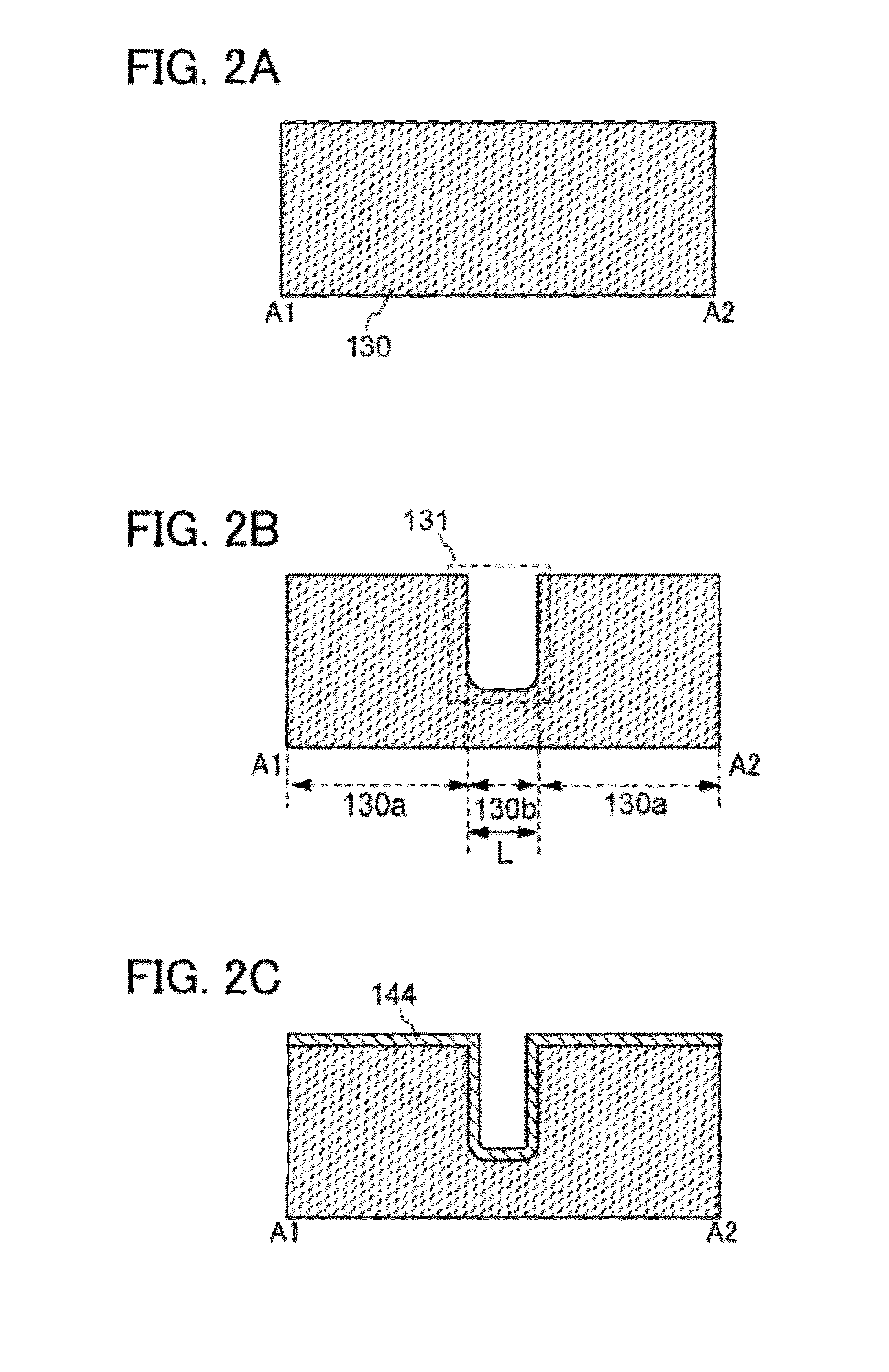
[0171]In this embodiment, another method for manufacturing the transistor 162 described in the above embodiment will be described with reference to FIGS. 2A to 2C and FIGS. 5A to 5C.

[0172]First, the insulating layer 130 is formed over a substrate (not illustrated) containing a semiconductor material (see FIG. 2A).

[0173]Next, the trench 131 is formed in the insulating layer 130 (see FIG. 2B).

[0174]Then, the oxide semiconductor film 144 is formed so as to be in contact with the bottom surface and the side surface of the trench 131 and the top surface of the first region 130a (see FIG. 5A).

[0175]The above embodiment can be referred to for the formation methods, materials, and the like of the insulating layer 130, the trench 131, and the oxide semiconductor film 144.

[0176]Next, a conductive layer is formed over the oxide semiconductor film 144 and is processed so that the source electrode 142a and the drain electrode 142b are formed (see FIG. 5B).

[0177]The above embodiment can be referr...

embodiment 3

[0196]In this embodiment, another method for manufacturing the transistor 162 described in the above embodiment will be described with reference to FIGS. 2A to 2C and FIGS. 6A to 6D.

[0197]First, the insulating layer 130 is formed over a substrate (not illustrated) containing a semiconductor material (see FIG. 2A).

[0198]Next, the trench 131 is formed in the insulating layer 130 (see FIG. 2B).

[0199]Then, the oxide semiconductor film 144 is formed so as to be in contact with the bottom surface and the side surface of the trench 131 and the top surface of the first region 130a (see FIG. 6A).

[0200]The above embodiment can be referred to for the formation methods, materials, and the like of the insulating layer 130, the trench 131, and the oxide semiconductor film 144.

[0201]Next, a resist mask 140 which covers the bottom surface of the trench 131 and the side surface of the trench 131, which excludes the upper end corner portion 131a, is formed in contact with and over the oxide semicondu...


PUM


Abstract

It is an object to provide a semiconductor device in which a short-channel effect is suppressed and miniaturization is achieved, and a manufacturing method thereof. A trench is formed in an insulating layer and impurities are added to an oxide semiconductor film in contact with an upper end corner portion of the trench, whereby a source region and a drain region are formed. With the above structure, miniaturization can be achieved. Further, with the trench, a short-channel effect can be suppressed setting the depth of the trench as appropriate even when a distance between a source electrode layer and a drain electrode layer is shortened.

Description

BACKGROUND OF THE INVENTION[0001]1. Field of the Invention[0002]The invention disclosed in this specification relates to a semiconductor device utilizing a semiconductor element and a manufacturing method thereof.[0003]2. Description of the Related Art[0004]Attention has been focused on a technique of using a semiconductor thin film formed over a substrate having an insulating surface to form a transistor. The transistor is applied to a wide range of electronic devices such as an integrated circuit (IC) or an image display device (display device). Further, a technique of using an oxide semiconductor for a semiconductor thin film that can be used for a transistor has been attracting attention.[0005]For example, it has been confirmed that an oxide semiconductor containing an In—Ga—Zn-based oxide is applicable to a channel formation region of a thin film transistor (Patent Document 1).REFERENCE[0006][Patent Document 1] Japanese Published Patent Application No. 2004-103957SUMMARY OF THE...

Claims


Application Information

Patent Timeline
Patent Type & Authority Patents(United States)
IPC IPC(8): H01L29/04H01L29/94H01L29/76H01L31/20H01L29/10H01L27/12H01L27/01H01L31/119H01L31/113H01L21/425H01L21/84H01L27/108H01L27/115H01L29/66H01L29/786H01L31/036H01L31/0376H01L31/0392H01L31/062H01L49/02
CPCH01L27/1156H01L27/1085H01L21/84H01L27/1225H01L27/1203H01L28/40H01L21/425H01L29/66742H01L27/10876H01L29/7869H01L21/02565H01L29/66969H01L21/265H01L29/66477H10B12/03H10B12/053H10B41/70H01L29/4238H01L29/78693H01L29/78603H01L29/045H01L29/0847
Inventor ISOBE, ATSUOSASAKI, TOSHINARIKOEZUKA, JUNICHIYAMAZAKI, SHUNPEI
Owner SEMICON ENERGY LAB CO LTD
Why Eureka
Try Eureka