Semiconductor storage device

a storage device and semiconductor technology, applied in the field of semiconductor storage devices, can solve the problems of difficult to perform high-speed write operations at 100 mhz or more, complicated current source circuits, and limited read speed of 2t1mtj cells, so as to achieve high-speed write operations and high-speed read operations without cell area overhead

Active Publication Date: 2011-08-30
NEC CORP
View PDF21 Cites 8 Cited by
  • Summary
  • Abstract
  • Description
  • Claims
  • Application Information

AI Technical Summary

Benefits of technology

[0016]An object of the present invention is to provide a semiconductor storage device using magnetoresistance effect elements, which can achieve high-speed operations (read operation and write operation) as in an SRAM (Static Random Access Memory).
[0017]Another object of the present invention is to provide a semiconductor storage device using a 2T1MTJ cell, which can achieve a high-speed read operation without cell area overhead, and perform a high-speed write operation.
[0020]The present invention allows performing a high-speed operation in a semiconductor storage device using a magnetoresistance element, as in an SRAM. The present invention also allows performing a high-speed read operation without cell area overhead in a semiconductor storage device using a 2T1MTJ cell, which can achieve a high-speed write operation.

Problems solved by technology

This complicates the current source circuit, and make it difficult to perform a high-speed write operation at 100 MHz or more.
However, a same read method as in the conventional MRAM is used, and therefore the operation speed of the 2T1MTJ cell is limited by the read speed.
Accordingly, the identification operation of the sense amplifier 105 cannot be performed before the sense signal and the reference signals are sufficiently settled, and therefore the read speed is limited.
Also, the variations in the power supply voltage, and the influence of capacitance coupling between interconnections are not constant, and therefore this technique is disadvantageous also in terms of the noise tolerance.
Accordingly, it is not easy to increase the read speed of the MRAM using the 2T1MTJ cell.
As a result, the operation speed of the MRAM, i.e., the random access time is limited by the read time of 10 ns or more.
However, the same writing method as in the conventional MRAM illustrated in FIG. 1 is used, and therefore the operation speed in this technique, i.e., the random access time is limited by a write time of 10 ns or more.
As described above, it is not easy to increase the operation speed (random access time) of the MRAM as that of the SRAM.
JP-A 2002-197852, for example, the cell area is increased to approximately 2 times, which is impractical.

Method used


Image

  • Semiconductor storage device
  • Semiconductor storage device
  • Semiconductor storage device

Examples


first embodiment

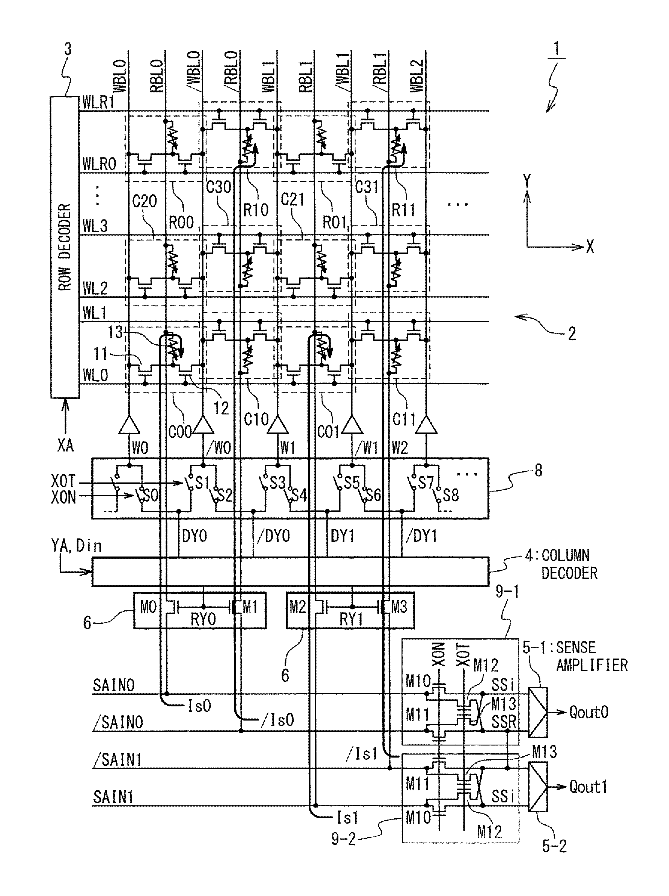
[0036]FIGS. 5 and 6 are circuit block diagrams illustrating a configuration of the semiconductor storage device in a first embodiment of the present invention. It should be noted that, in FIG. 5, a path of a sense current in a read operation is also illustrated. In FIG. 6, a path of a write current in a write operation is also illustrated.

[0037]The semiconductor storage device 1 is a 2T1MTJ cell type MRAM. The semiconductor storage device 1 includes a memory array 2, a row decoder 3, a column decoder 4, a sense amplifier 5, a first switch section 6, a second switch section 8, and a selector 9.

[0038]The memory array 2 includes: a plurality of word lines WLi (i=0 to n: n is a natural number); a plurality of read bit lines RBLj and / RBLj (j=1 to m: m is a natural number); a plurality of write bit lines WBLj and / WBLj; a plurality of memory cells Cij (i=0 to n, j=0 to m); two reference word lines WLR0 and WLR1; and a plurality of reference cells R0j and R1j (j=0 to m). It should be note...

second embodiment

[0104]FIG. 14 is a circuit block diagram illustrating a configuration in a second embodiment of the semiconductor storage device of the present invention. It should be noted that the path of the sense current in the read operation is also illustrated in FIG. 14.

[0105]In order to further reduce the load capacitance of a read bit line RBL, this embodiment is designed differently from the first embodiment in that the memory array 2 is divided into a plurality of memory arrays 2-r (r=0 to p: p is a natural number). It should be noted that, in this embodiment, the arrangement of the memory cells C and the write operation in each memory array 2-r are the same as those in the first embodiment, and therefore descriptions thereof are omitted. It should be also noted that although the description is given of FIG. 5 on an assumption that two memory cells C are simultaneously selected, it is assumed in FIG. 14 that one memory cell C is selected for convenience of description.

[0106]The semicondu...


PUM


Abstract

A semiconductor storage device is provided with a memory array including a plurality of memory cells. The plurality of memory cells includes: first and third memory cells arranged along one of an even-numbered row and an odd-numbered row, and a second memory cell arranged along the other. Each of the plurality of memory cells includes: a first transistor comprising first and second diffusion layers; a second transistor comprising third and fourth diffusion layers; and a magnetoresistance element having one of terminals thereof connected to an interconnection layer which provides an electrical connection between the second and third diffusion layers. The fourth diffusion layer of the first memory cell is also used as the first diffusion layer of the second memory cell. In addition, the fourth diffusion layer of the second memory cell is also used as the first diffusion layer of the third memory cell.

Description

[0001]This application is the National Phase of PCT / JP2008 / 052059, filed Feb. 7, 2008, which is based upon and claims priority from Japanese Patent Application No. 2007-041204 filed Feb. 21, 2007.TECHNICAL FIELD[0002]The present invention relates to a semiconductor storage device, and more particularly, to a semiconductor storage device in which a magnetoresistance element (MTJ: Magnetic Tunnel Junction) is incorporated into a memory cell as a memory element, i.e., a magnetic random access memory (MRAM). This application claims priority based on Japanese patent application No. 2007-041204, the disclosure of which is incorporated herein by reference.BACKGROUND ART[0003]An MTJ element used for a memory cell of an MRAM includes a fixed magnetic layer, a free magnetic layer, and a tunnel insulating film. In the fixed magnetic layer, the direction of the magnetization is fixed to an arbitrary direction. In the free magnetic layer, the direction of the magnetization is changeable by an ex...

Claims


Application Information

Patent Timeline
Patent Type & Authority Patents(United States)
IPC IPC(8): G11C11/00
CPCB82Y10/00B82Y25/00G11C11/16H01L27/228H01L43/08G11C11/1655G11C11/1673G11C11/1659G11C11/1675H10B61/22H10N50/10
Inventor SAKIMURA, NOBORUHONDA, TAKESHISUGIBAYASHI, TADAHIKO
Owner NEC CORP
Why Eureka
Try Eureka