Methods of forming NAND memory with virtual channel

Active Publication Date: 2009-02-24
SANDISK TECH LLC
View PDF16 Cites 29 Cited by
  • Summary
  • Abstract
  • Description
  • Claims
  • Application Information

AI Technical Summary

Problems solved by technology

However, the development of the many electronic card standards has created different types of cards that are incompatible with each other in various degrees.

Method used


Image

  • Methods of forming NAND memory with virtual channel
  • Methods of forming NAND memory with virtual channel
  • Methods of forming NAND memory with virtual channel

Examples


Embodiment Construction

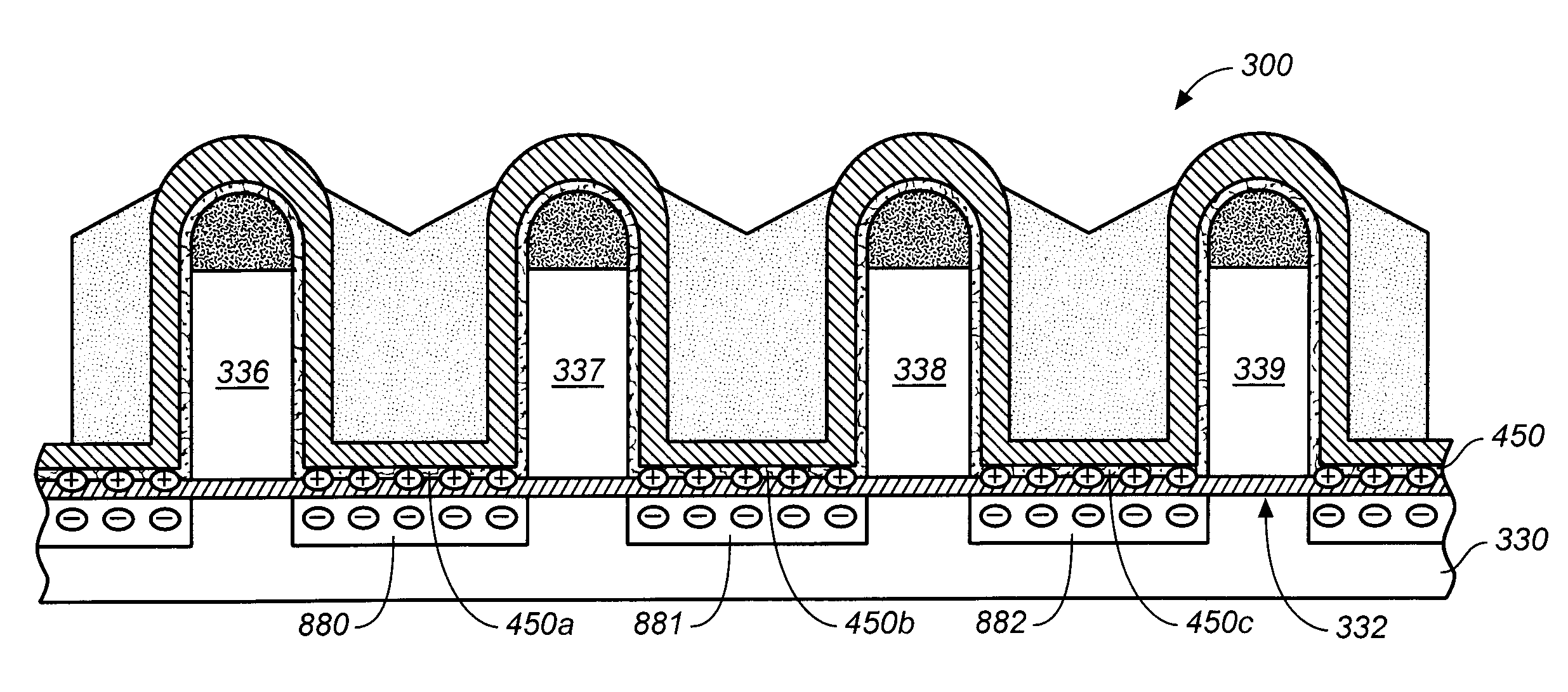
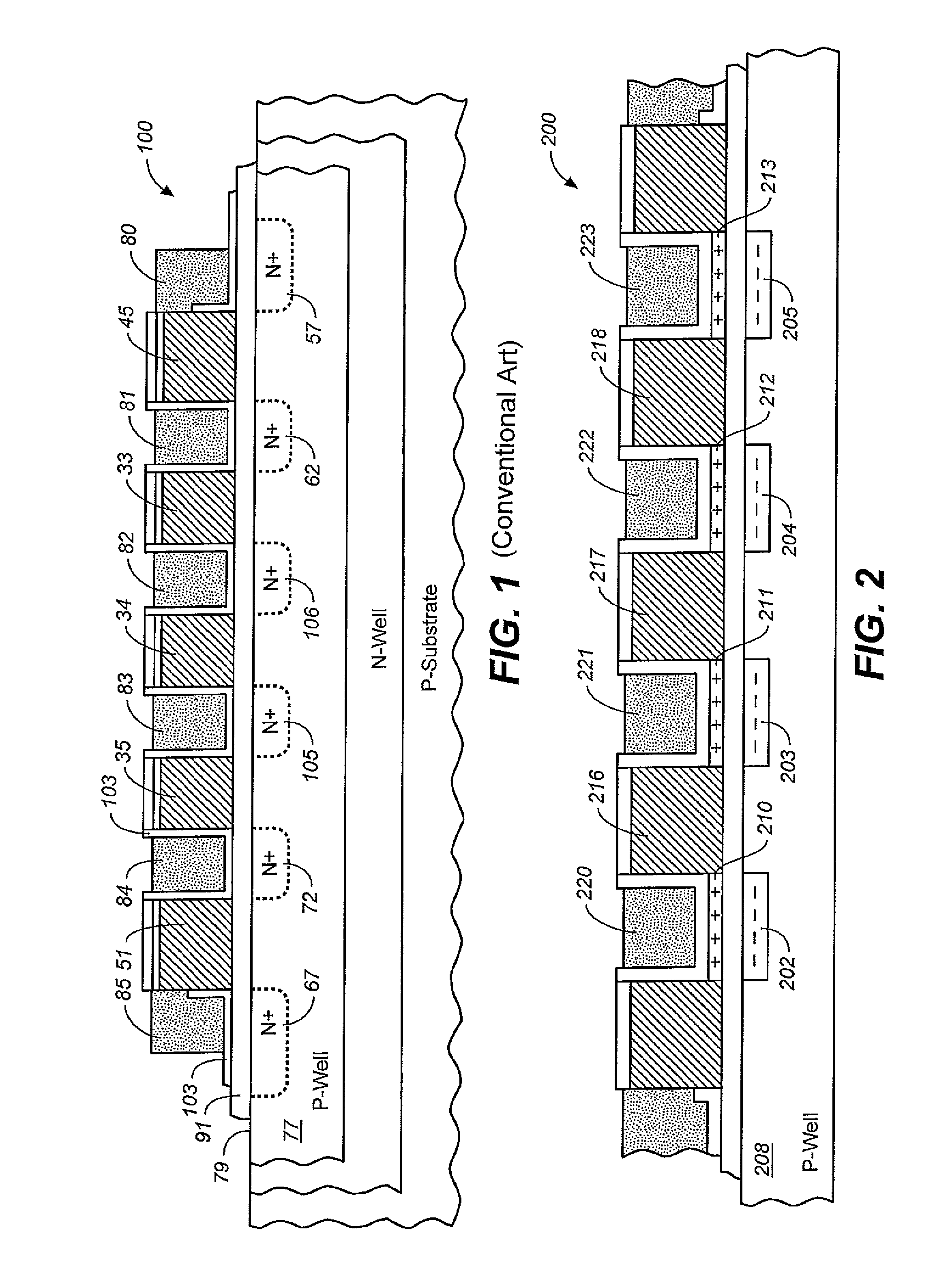
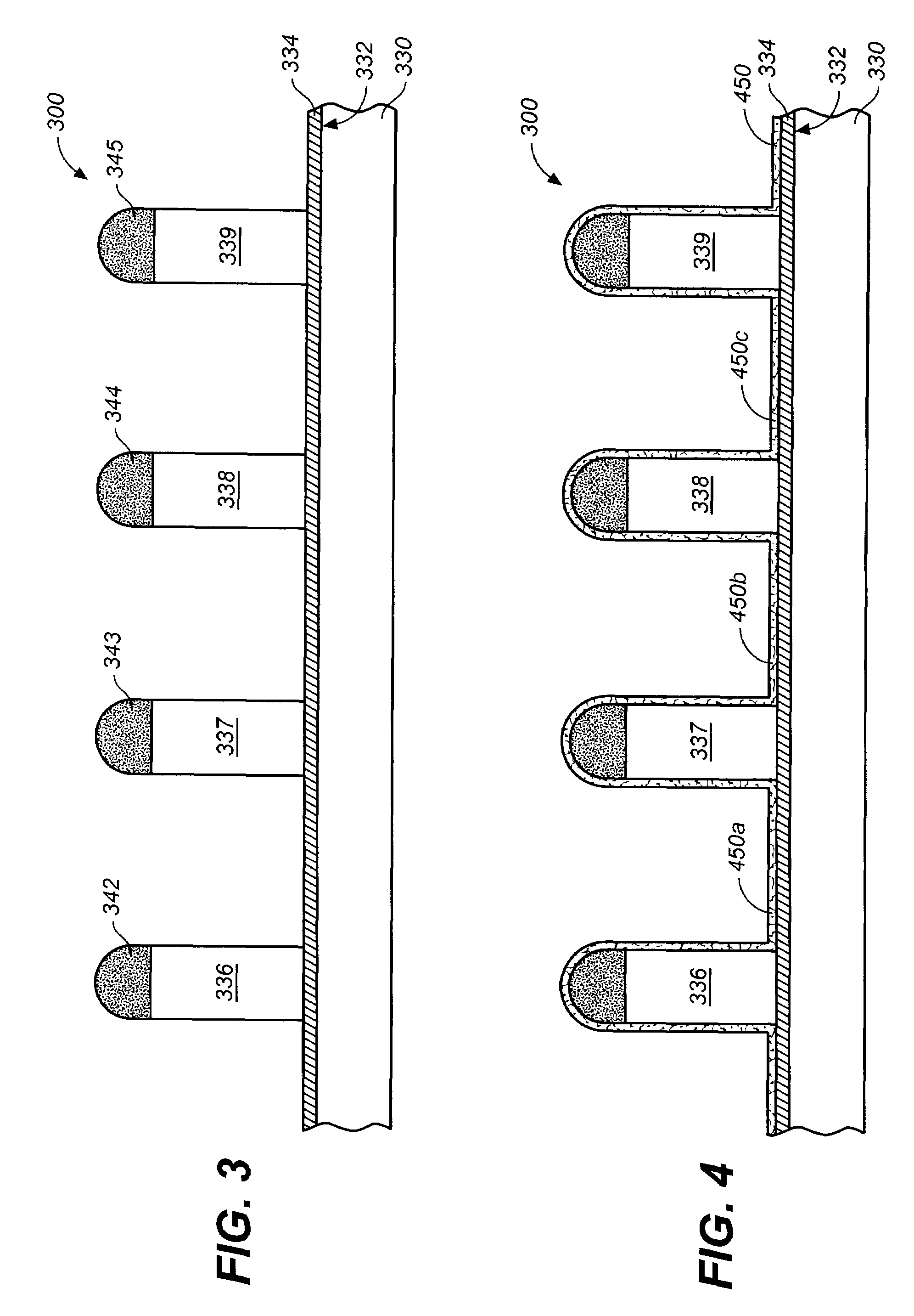
[0018]FIG. 1 shows a cross section of a NAND flash memory string 100 that has control gates 81-84 extending on both sides of floating gates 33-35 (this type of array is sometimes referred to as ENAND). Examples of such strings and methods of forming them are described in U.S. Pat. No. 6,888,755. In string 100 of FIG. 1 a floating gate is coupled to two control gates, one on either side of the control gate (e.g. floating gate 34 is coupled to control gates 82 and 83). This is in contrast to a common memory design where a control gate overlies a floating gate so that each floating gate is coupled to only one control gate. A memory string such as that of FIG. 1 may be formed as part of a memory array having many strings. Neighboring strings may be isolated from each other by Shallow Trench Isolation (STI) structures, or other means (not shown in FIG. 1). In some cases, individual stings may have 8, 16, 32 or more memory cells connected together in series. Select gates 45, 51 are provid...


PUM


Abstract

A string of nonvolatile memory cells are connected together by source / drain regions that include an inversion layer created by fixed charge in an overlying layer. Control gates extend between floating gates so that two control gates couple to a floating gate. A fixed charge layer may be formed by plasma nitridation.

Description

CROSS-REFERENCE TO RELATED APPLICATIONS[0001]This application claims the benefit of U.S. provisional patent application No. 60 / 884,863, filed on Jan. 12, 2007. This application is related to U.S. patent application Ser. No. 11 / 626,778, filed Jan. 24, 2007, entitled, “NAND Memory with Virtual Channel”; These applications are incorporated in their entirety by reference as if fully set forth herein.BACKGROUND OF THE INVENTION[0002]This invention relates to nonvolatile memories and methods of forming nonvolatile memories. In particular, this application relates to nonvolatile memory arrays in which a series of floating gate memory cells are electrically connected in series.[0003]Nonvolatile memory systems are used in various applications. Some nonvolatile memory systems are embedded in a larger system such as a personal computer. Other nonvolatile memory systems are removably connected to a host system and may be interchanged between different host systems. Examples of such removable me...

Claims


Application Information

Patent Timeline
Patent Type & Authority Patents(United States)
IPC IPC(8): H01L21/336
CPCH01L27/115H01L27/11521H01L27/11524H10B41/35H10B69/00H10B41/30
Inventor CHIEN, HENRYMATAMIS, GEORGEORIMOTO, TAKASHIKAI, JAMES
Owner SANDISK TECH LLC
Why Eureka
Try Eureka