Method for manufacturing a solid-state image capturing element

a solid-state image and manufacturing method technology, applied in the direction of chemical vapor deposition coating, radiation control devices, coatings, etc., can solve the problems of picture quality deterioration and signal deterioration, and achieve the effect of preventing deterioration of picture quality, reducing signal deterioration, and increasing fine white defects

Inactive Publication Date: 2011-06-30
SHARP KK
View PDF10 Cites 19 Cited by
  • Summary
  • Abstract
  • Description
  • Claims
  • Application Information

AI Technical Summary

Benefits of technology

[0029]As a result, the deposition temperature of the interlayer insulation film, or the HDP film, can be controlled to 365° C. or below, preferably within a temperature range of 335° C. to 365° C., and more preferably 335° C. to 350° C., or at 350° C. Thus, it becomes possible to suppress signal deterioration due to dark current and an increase in fine white defects, and to prevent deterioration of picture quality, even when the HDP film with a favorable embedding capability between fine wiring is used as an interlayer insulation film.
[0030]In addition, as the RF power indicating a plasma generation energy is raised to 850 W to 900 W and further to 930 W and higher, the amount of hydrogen separated from the plasma SiN film at a low temperature will increase at a later-performed sintering process, thus performing the sintering process reliably. As a result, on the surface of the light receiving elements, it becomes possible to reliably repair a defect on a silicon surface, which was caused by plasma dry etching of a metal layer, to suppress dark current even further. In addition, since the lowering of a film transmissivity of the passivation film with...

Problems solved by technology

In the conventional technique described above, however, there are following problems: when an HDP film, which is favorably embedded between lines, is used as an interlayer insulation film, as wire l...

Method used


Image

  • Method for manufacturing a solid-state image capturing element
  • Method for manufacturing a solid-state image capturing element
  • Method for manufacturing a solid-state image capturing element

Examples


embodiment 1

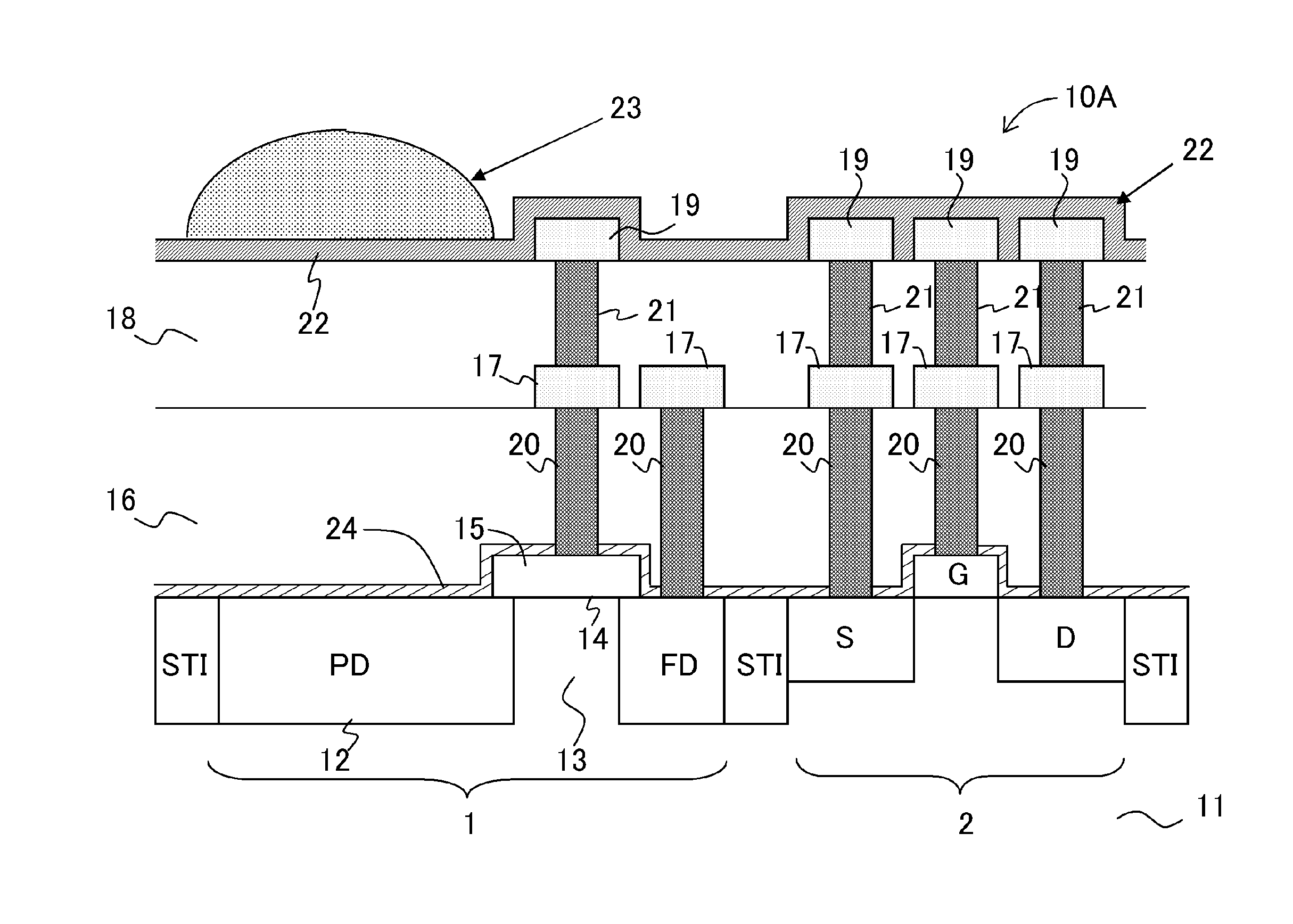
[0074]FIG. 1 is a longitudinal cross sectional view schematically illustrating an exemplary essential part structure of a CMOS solid-state image capturing element according to Embodiment 1 of the present invention.

[0075]In FIG. 1, a photodiode 12 is formed as a surface layer of a semiconductor substrate 11 in each pixel section 1 of a CMOS solid-state image capturing element 10 according to Embodiment 1. The photodiode 12 functions as a photoelectric conversion section (light receiving element) for each pixel. Adjacent to the photodiode 12, an electric charge transfer section 13 is provided in an electric charge transfer transistor for transferring a signal charge to a floating diffusion section (electric charge voltage converting section) FD. Above the electric charge transfer section 13, a transfer gate 15 is provided with a gate insulation film 14 interposed therebetween, the transfer gate 15 functioning as a lead electrode. With the electric charge transfer section 13, gate insu...

embodiment 2

[0101]Embodiment 1 described above is a case where after an aluminum (Al) wiring pattern in the upper most layer is formed and before a color filter is formed, the plasma silicon nitride film 22 is formed and a sintering process is performed. In Embodiment 2, a case will be described in detail where together with such steps, a plasma SiN film 24 to be described later is formed on a front surface side of the photodiode 12 with a gate insulation film 14, which is an oxide film, interposed therebetween, and a sintering process is performed.

[0102]FIG. 6 is a longitudinal cross sectional view schematically illustrating an exemplary essential part structure of a CMOS solid-state image capturing element according to Embodiment 2 of the present invention. In FIG. 6, the members having the same function and effect as the corresponding ones of the CMOS solid-state image capturing element 10 in FIG. 1 are added with the same reference numerals to be described.

[0103]In FIG. 6, a photodiode 12 i...

embodiment 3

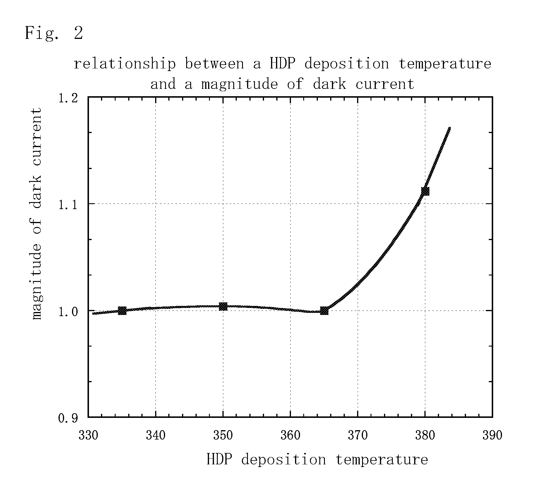
[0121]In Embodiments 1 and 2 described above, the case has been described where the present invention, in which the deposition temperature of the HDP films 16 and 18 is controlled at 365° C. or below, is applied to a CMOS solid-state image capturing element. In Embodiment 3, a case will be described where the present invention, in which the deposition temperature of the HDP films 16 and 18 is controlled at 365° C. or below, is applied to a CCD solid-state image capturing element.

[0122]FIG. 7 is a longitudinal cross sectional view schematically illustrating an exemplary essential part structure of a CCD solid-state image capturing element according to Embodiment 3 of the present invention.

[0123]In FIG. 7, in each pixel section of a CCD solid-state image capturing element 30 according to Embodiment 3, a photodiode 32 is provided in a semiconductor substrate 31, the photodiode 32 being for performing a photoelectric conversion on incident light and generating a signal electric charge a...


PUM

PropertyMeasurementUnit
Temperatureaaaaaaaaaa

Abstract

The deposition temperature of the HDP film can be controlled to 365° C. or below, preferably within a temperature range of 335° C. to 365° C., and more preferably 335° C. to 350° C., or at 350° C. Thus, it becomes possible to suppress signal deterioration due to dark current and an increase in fine white defects, and to prevent deterioration of picture quality, even when the HDP film with a favorable embedding capability between fine wiring is used as an interlayer insulation film. An RF power is set to 850 W to 1500 W, so that dark current can be suppressed even more. Further, a plasma silicon nitride film with a refractive index of 1.9 or more and 2.15 or less for a blue wavelength is formed, so that it becomes possible to suppress the lowering of a blue sensitivity in the light receiving elements to further improve picture quality.

Description

[0001]This nonprovisional application claims priority under 35 U.S.C. §119(a) to Patent Application No. 2009-286990 filed in Japan on Dec. 17, 2009, the entire contents of which are hereby incorporated by reference.BACKGROUND OF THE INVENTION[0002]1. Field of the Invention[0003]The present invention relates to a method for manufacturing a solid-state image capturing element, which is constituted of semiconductor elements for performing a photoelectric conversion on and capturing an image of image light from a subject.[0004]2. Description of the Related Art[0005]Conventional solid-state image capturing elements of this type are used, for example, for an electronic information device, such as a digital camera (e.g. a digital video camera or a digital still camera), an image input camera (e.g. a monitoring camera), a scanner, a facsimile machine, a television telephone device, and a camera-equipped cell phone device. In the conventional solid-state image capturing elements, a SiN film ...

Claims


Application Information

Patent Timeline
IPC IPC(8): H01L31/18H01L31/0232
CPCC23C16/345C23C16/505C23C16/52C23C16/56H01L27/14818H01L27/14643H01L27/14687H01L27/148H01L27/14623
Inventor SUEYOSHI, YASUHIKO
Owner SHARP KK
Why Eureka
Try Eureka