Semiconductor nonvolatile memory device, and manufacturing method thereof

a non-volatile memory and semiconductor technology, applied in the direction of semiconductor devices, basic electric elements, electrical appliances, etc., can solve the problems of easy leak current to flow through and easy damage of nitride film by plasma, so as to reduce the damage caused by plasma, and strengthen the tunnel insulating film further

Inactive Publication Date: 2006-07-27
RENESAS TECH CORP
View PDF3 Cites 20 Cited by
  • Summary
  • Abstract
  • Description
  • Claims
  • Application Information

AI Technical Summary

Benefits of technology

[0013] According to the first aspect of the present invention, the surface of the silicon oxide film is radically nitrided, so that the first silicon nitride oxide film is formed. The film formed by a radical nitriding process makes it difficult for defects to occur in the film, in comparison with a nitride film formed by a CVD method. In addition, the radical nitriding process can reduce damage caused by plasma, in comparison with a conventional simple plasma nitriding process. It is therefore possible to manufacture a semiconductor nonvolatile memory device where a leak current does not easily flow through a tunnel insulating film.
[0014] According to the second aspect of the present invention, the silicon nitride oxide film constituting the tunnel insulating film is formed by radically nitriding the surface of the silicon oxide film. The film formed by a radical nitriding process makes it difficult for defects to occur in the film, in comparison with a nitride film formed by a CVD method. In addition, the radical nitriding process can reduce damage caused by plasma, in comparison with a conventional simple plasma nitriding process. It is therefore possible to obtain a semiconductor nonvolatile memory device where a leak current does not easily flow through a tunnel insulating film.
[0015] According to the third aspect of the present invention, the tunnel insulating film is constituted by the silicon oxide film as well as the first and second silicon nitride oxide films. The second silicon nitride oxide film is formed between the silicon oxide film and the semiconductor substrate. Therefore, defects do not easily occur in the interface between the tunnel insulating film and the semiconductor substrate. It is possible to obtain a semiconductor nonvolatile memory device where an interface state in the interface between the tunnel insulating film and the semiconductor substrate does not easily increase. Accordingly, the tunnel insulating film can further be strengthened; thus, it is possible to obtain a semiconductor nonvolatile memory device where a leak current does not easily flow through the tunnel insulating film.

Problems solved by technology

If the nitride film portion of a tunnel insulating film of a semiconductor nonvolatile memory device is formed by a CVD method, defects easily occur in the nitride film.
In addition, if a nitride film portion of a tunnel insulating film is formed by a simple plasma nitriding process, the nitride film is easily damaged by plasma.
When aforementioned defects or damages occur in the nitride film, it becomes easy for a leak current to flow through the tunnel insulating film.
Even when a nitride film is additionally formed on the silicon oxide film, reduction in the rate of data erasure in the semiconductor nonvolatile memory device due to an increase in the interface state in the interface between the oxide film portion and the semiconductor substrate such as the silicon substrate does not improve.

Method used


Image

  • Semiconductor nonvolatile memory device, and manufacturing method thereof
  • Semiconductor nonvolatile memory device, and manufacturing method thereof
  • Semiconductor nonvolatile memory device, and manufacturing method thereof

Examples


first embodiment

[0028] A first embodiment is directed to a semiconductor nonvolatile memory device where a silicon nitride oxide film that constitutes a tunnel insulating film is formed by radically nitriding a surface of a silicon oxide film, and a manufacturing method thereof.

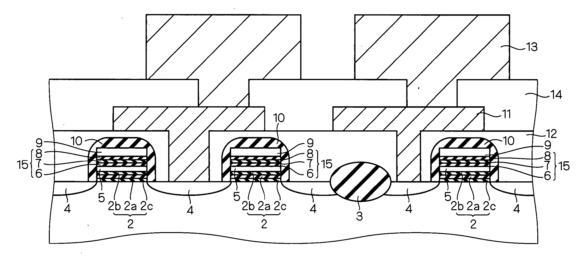
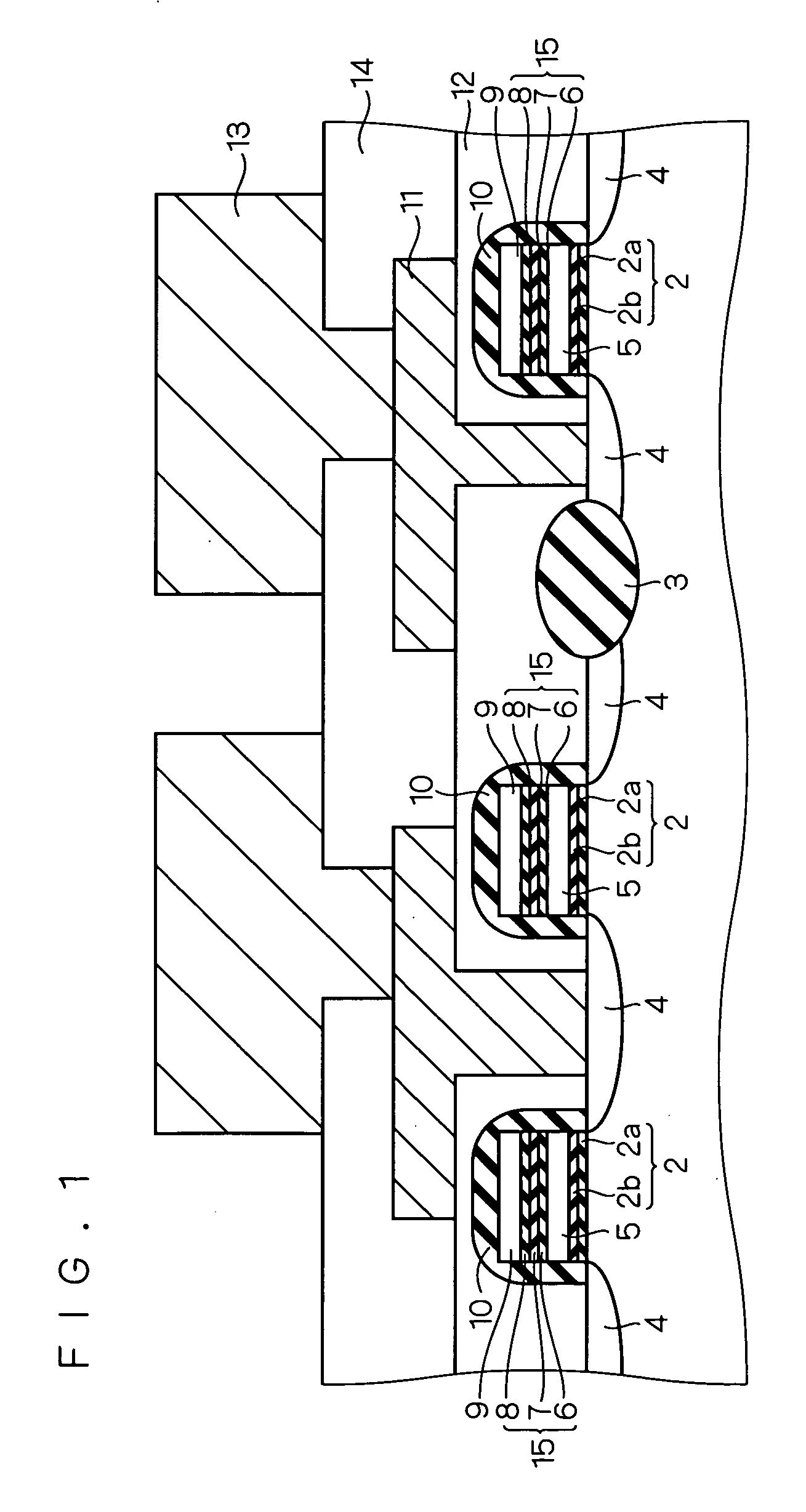
[0029]FIG. 1 shows the semiconductor nonvolatile memory device according to this embodiment. As shown in FIG. 1, this semiconductor nonvolatile memory device includes a semiconductor substrate 1 such as a silicon substrate.

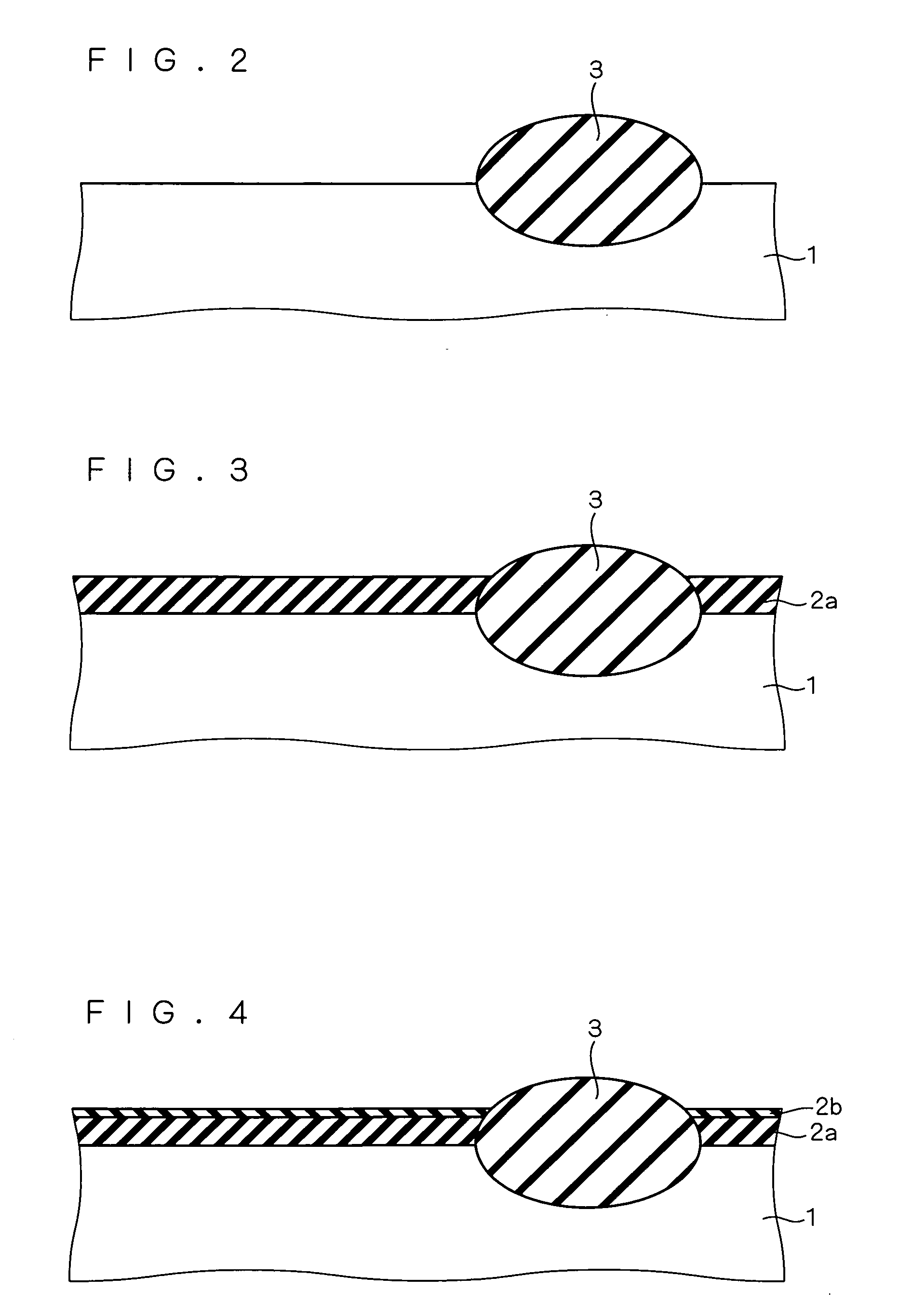
[0030] An element isolation region 3 of which the main component is a silicon oxide film, and source / drain regions 4 which are components of the semiconductor nonvolatile memory device are formed on a surface of the semiconductor substrate 1. Here, the source / drain regions 4 are active regions which are formed by selectively making n-type impurities such as phosphorous or arsenic diffuse into portions on the surface of the semiconductor substrate 1.

[0031] Silicon oxide films 2a are formed on the semicon...

second embodiment

[0051] A second embodiment is directed to modifications of the semiconductor nonvolatile memory device and the manufacturing method thereof according to the first embodiment, where additional silicon nitride oxide films which constitute the tunnel insulating film 2 are formed between the silicon oxide films 2a and the semiconductor substrate 1 according to the first embodiment.

[0052]FIG. 7 shows a semiconductor nonvolatile memory device according to this embodiment. As shown in FIG. 7, this semiconductor nonvolatile memory device is different from the semiconductor nonvolatile memory device of FIG. 1 in the following point. That is, this semiconductor nonvolatile memory device includes additional silicon nitride oxide films 2c which are formed between the semiconductor substrate I and the silicon oxide films 2a. In addition, each layered film which is constituted by the silicon oxide film 2a and the silicon nitride oxide films 2b and 2c functions as a tunnel insulating film 2 of on...


PUM

PropertyMeasurementUnit
pressureaaaaaaaaaa
temperatureaaaaaaaaaa

Abstract

The present invention realizes a semiconductor nonvolatile memory device where a leak current does not easily flow through a tunnel insulating film, and a manufacturing method thereof A silicon nitride oxide film constituting a tunnel insulating film is formed by radically nitriding a surface of a silicon oxide film. The film formed by a radical nitriding process makes it difficult for defects to occur in the film, in comparison with a nitride film formed by a CVD method. In addition, the radical nitriding process causes less plasma damage, in comparison with a conventional simple plasma nitriding process. It is therefore possible to obtain a semiconductor nonvolatile memory device where a leak current does not easily flow through a tunnel insulating film.

Description

BACKGROUND OF THE INVENTION [0001] 1. Field of the Invention [0002] The present invention relates to a semiconductor nonvolatile memory device having a tunnel insulating film, and a manufacturing method thereof. [0003] 2. Description of the Background Art [0004] In a third embodiment of Japanese Patent Application Laid-Open No. 11-317463 (1999), there is described a tunnel insulating film 1 of a semiconductor nonvolatile memory device which has a layered structure of a thermal oxide film 21 and a nitride film 23 formed by a CVD (Chemical Vapor Deposition) method. [0005] In addition, in paragraph “0026” of Japanese Patent Application Laid-Open No. 2004-47614, there is described a tunnel insulating film 15a of a semiconductor nonvolatile memory device, which is constituted by a layered film where a plasma nitride film is layered on a plasma oxide film. [0006] If the nitride film portion of a tunnel insulating film of a semiconductor nonvolatile memory device is formed by a CVD method,...

Claims


Application Information

Patent Timeline
Patent Type & Authority Applications(United States)
IPC IPC(8): H01L21/336H01L21/31
CPCH01L21/28202H01L21/3144H01L27/115H01L27/11521H01L29/513H01L29/518H01L21/0214H01L21/02312H10B69/00H10B41/30H01L21/02332
Inventor KANEOKA, TATSUNORIMARUYAMA, YOSHIKIYAMAMOTO, SATOSHIUENISHI, TOSHIYA
Owner RENESAS TECH CORP
Why Eureka
Try Eureka