Method of manufacturing multilayer optical information recording medium
a multi-layer optical information and recording medium technology, applied in the field of manufacturing multi-layer optical information recording mediums, can solve problems such as deterioration s/n, and achieve the effect of maintaining the shape of the (k1)th stamper or the kth signal substra
- Summary
- Abstract
- Description
- Claims
- Application Information
AI Technical Summary
Benefits of technology
Problems solved by technology
Method used
Image

Examples
embodiment 1
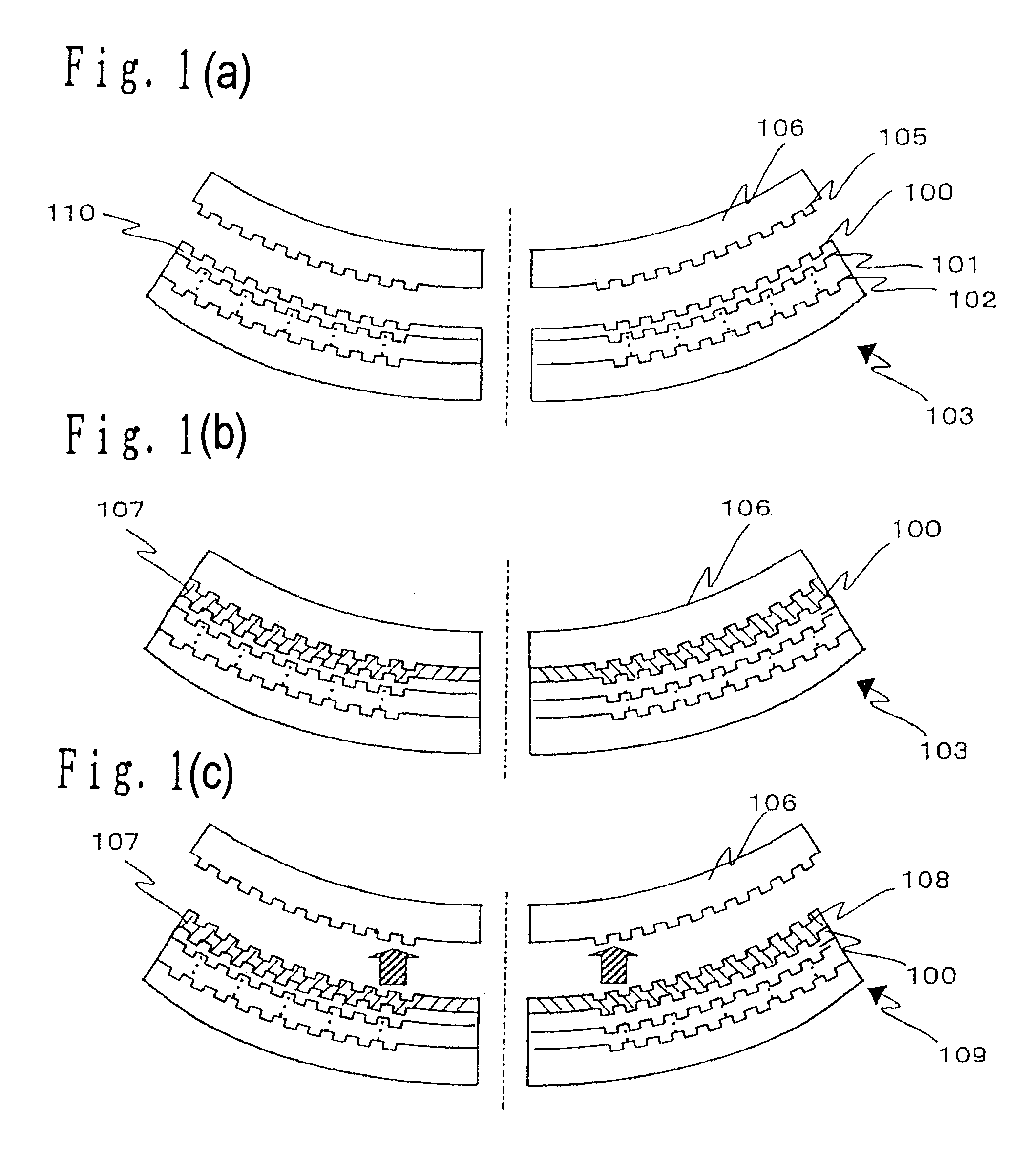
[0189]FIGS. 1(a)-1(c) show an embodiment of a method of manufacturing a multilayer optical information recording medium according to the present invention. FIGS. 1(a)-1(c) are schematic views of a step of forming a (k−1)th separation layer 107 between a kth signal recording layer 100 and a (k−1)th signal recording layer of a disk type multilayer optical information recording medium having n (n: 2 or more) signal recording layers and a separation layer between the respective signal recording layers recording and reproducing information to / from one side. Here, suppose the kth signal recording layer 100 is the kth (k: 2 or above and n or below) signal recording layer from the recording / reproduction surface and a substrate having the kth signal recording layer 100 on the surface is a kth signal substrate 103. Furthermore, suppose the stamper having guide grooves and pits 105 of the (k−1)th signal recording layer is a (k−1)th stamper 106.
[0190]The step of forming a (k−1)th separation lay...
embodiment 2
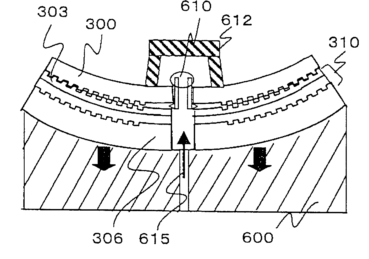
[0228]Embodiment 2 of the method of manufacturing a multilayer optical information recording medium according to the present invention will be explained. FIGS. 9(a)-8(c) show a case with warpage opposite to that in Embodiment 1, that is, a case where the kth signal substrate is warped so as to wrap around the surface opposite to the kth signal recording layer. As with FIGS. 1(a)-1(c), both the kth signal substrate and the (k−1)th stamper in FIGS. 8(a)-8(c) have a disk shape and have a central hole in the center.
[0229]First, as shown in FIG. 8(a), the kth signal substrate 803 is provided with not only the kth signal recording layer 800 on the surface of the kth separation layer 810 but also a total of (n-k−1) signal recording layers from the (k−1)th signal recording layer 801 to the nth signal recording layer 802. As in the case of Embodiment 1, the signal recording layer consists of guide grooves for guiding recording light or reproducing light when information is recorded in or rep...
embodiment 3
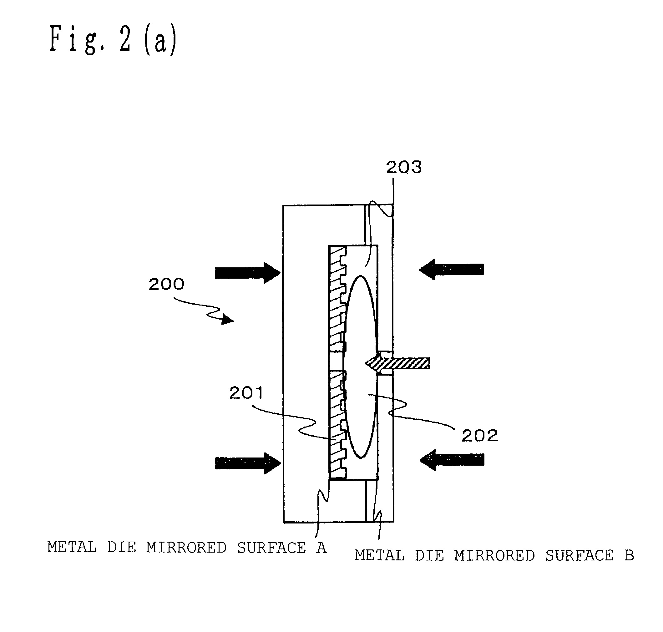
[0249]Here, an alternative method for the method of manufacturing the (k−1)th stamper shown in FIGS. 2(a)-2(b) will be explained. FIGS. 12(a)-12(b) are schematic views of a molding metal die provided with a heat insulator. This is intended to warp the (k−1)th stamper so as to wrap around the surface opposite to the surface on which guide grooves and pits are provided.
[0250]FIG. 12(a) shows a case where a heat insulator 1200 is provided between a master stamper 201 and a metal die mirrored surface A. Cooling water flows through a cooling water channel A and a cooling water channel B to cool melted polycarbonate 202 introduced inside a cavity 203 of a molding metal die 200. By inserting the heat insulator 1200, the metal die mirrored surface B side is cooled according to the temperature of the cooling water that flows through the cooling water channel B, while for the master stamper 201 side, the temperature of the melted polycarbonate 202 is hardly cooled and therefore the master sta...
PUM
| Property | Measurement | Unit |
|---|---|---|
| Thickness | aaaaa | aaaaa |
| Pressure | aaaaa | aaaaa |
| Viscosity | aaaaa | aaaaa |
Abstract
Description
Claims
Application Information
 - Generate Ideas
- Intellectual Property
- Life Sciences
- Materials
- Tech Scout
- Unparalleled Data Quality
- Higher Quality Content
- 60% Fewer Hallucinations
Browse by: Latest US Patents, China's latest patents, Technical Efficacy Thesaurus, Application Domain, Technology Topic, Popular Technical Reports.
© 2025 PatSnap. All rights reserved.Legal|Privacy policy|Modern Slavery Act Transparency Statement|Sitemap|About US| Contact US: help@patsnap.com