
PLL circuit and high-frequency receiving device

a high-frequency receiving and circuit technology, applied in the direction of digital transmission, generating/distributing signals, baseband system details, etc., can solve the problem of taking time to set a cycle, and achieve the effect of shortening the tim

Inactive Publication Date: 2009-03-24
SHARP KK
View PDF19 Cites 3 Cited by
  • Summary
  • Abstract
  • Description
  • Claims
  • Application Information

AI Technical Summary

Benefits of technology

This approach significantly reduces the time needed to set a cycle in PLL circuits, even for high-frequency receiving devices, ensuring efficient reception by minimizing the time required for cycle setting and allowing for convenient selection of set cycles based on channel conditions.

Problems solved by technology

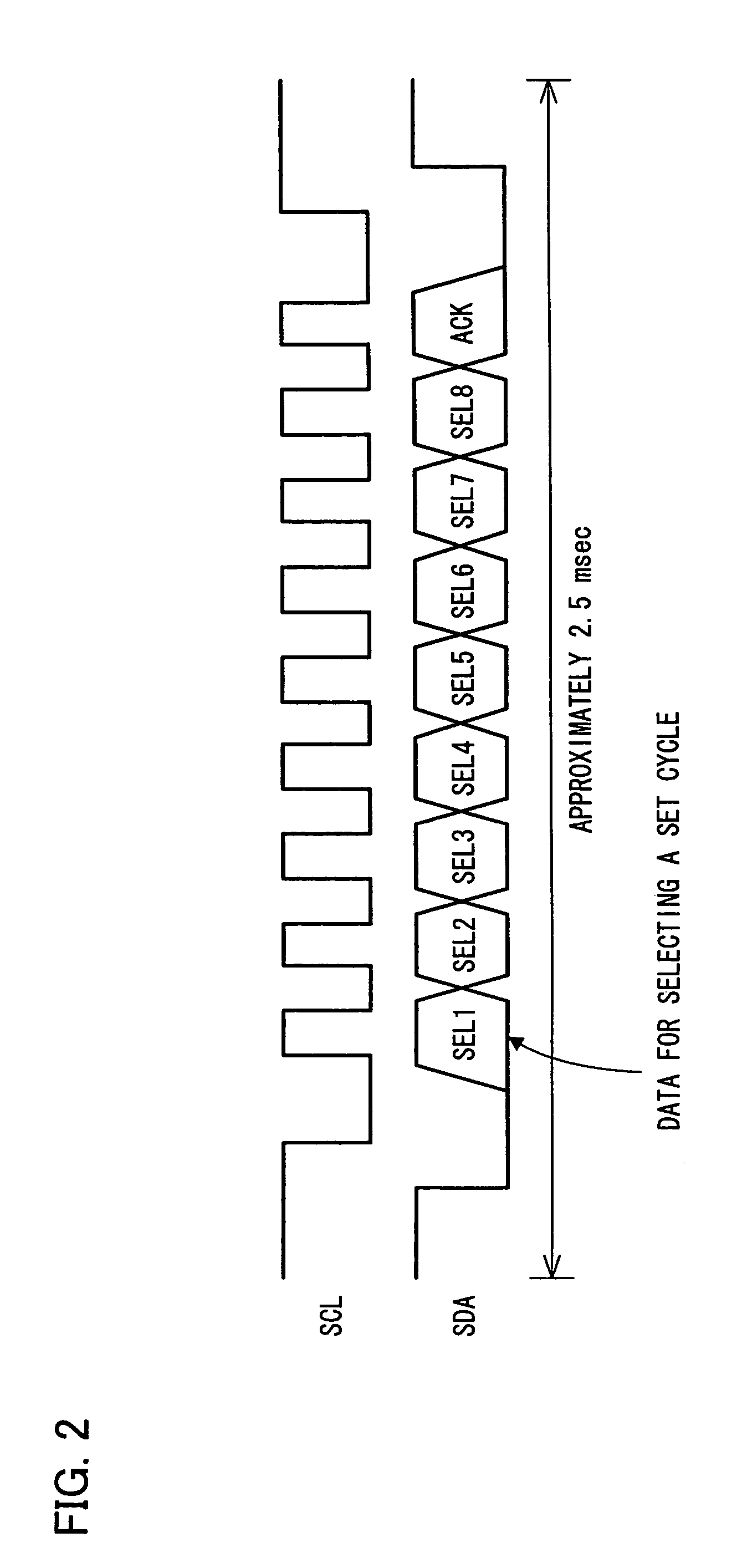
However, since the set cycle is usually inputted through a serial bus, there is such a problem that it takes time to set a cycle.

Method used


Image

  • PLL circuit and high-frequency receiving device
  • PLL circuit and high-frequency receiving device
  • PLL circuit and high-frequency receiving device

Examples


first embodiment

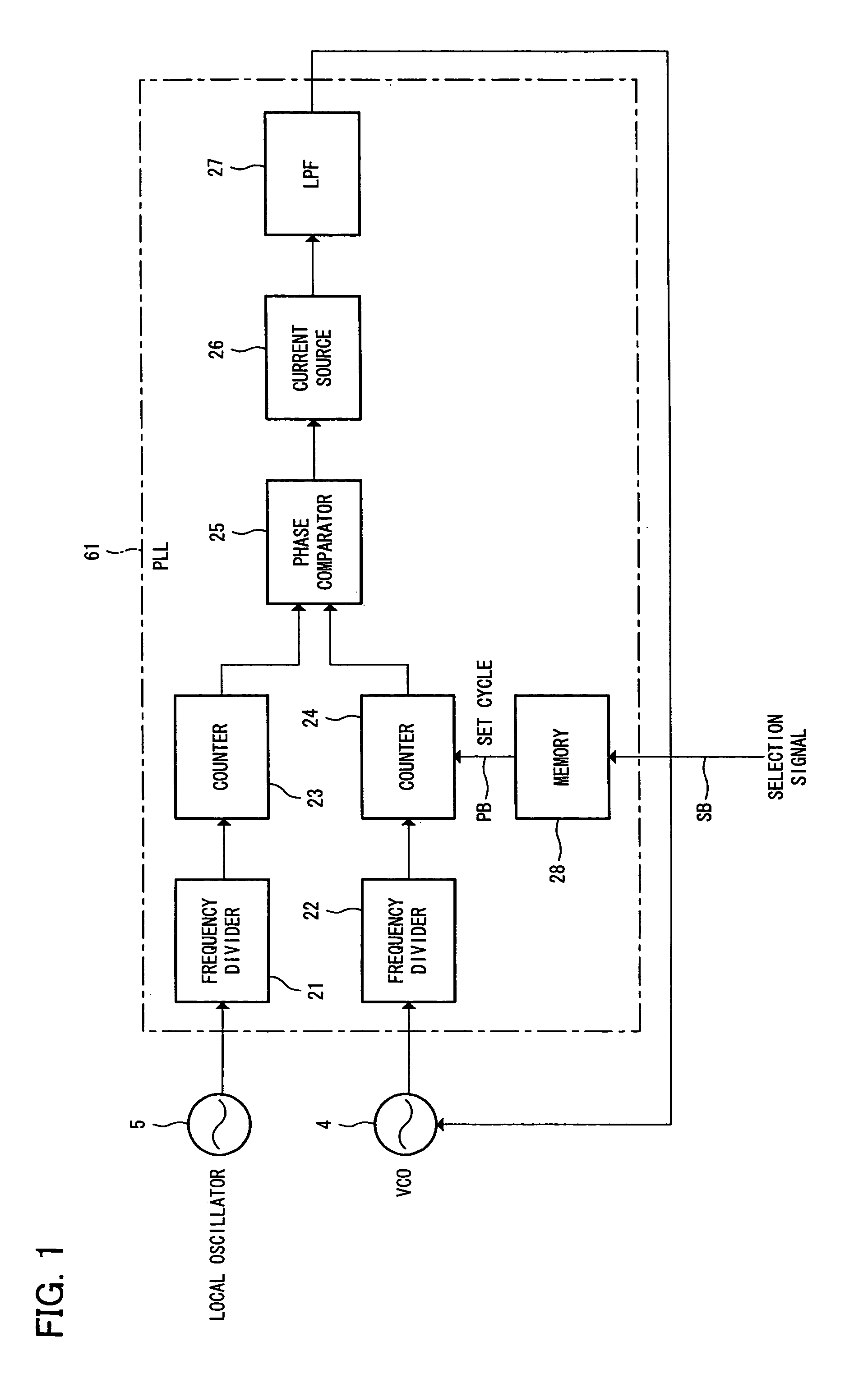
[0036]FIG. 1 is a block diagram illustrating an arrangement of a PLL circuit 61 according to the present embodiment.

[0037]As illustrated in FIG. 1, the PLL circuit 61 has frequency dividers 21 and 22, counters 23 and 24, a phase comparator 25, a current source 26, a low-pass filter (LPF) 27, and a memory 28.

[0038]The frequency divider 21 divides at a predetermined frequency-dividing ratio a frequency signal, outputted from a local oscillator 5, which serves as a reference of a local signal outputted by a voltage-control local oscillator (VCO) 4. The frequency divider 22 divides at a predetermined frequency-dividing ratio an output signal from the voltage-control local oscillator (VCO) 4. In order to make it easy for the counters 23 and 24 to count, the frequency divider 22 functions as a prescaler which divides in advance an output of the high-frequency local oscillator 5 and an output of the VCO 4.

[0039]The counter 23 counts down (or counts up) the frequency-divided signal divided ...

second embodiment

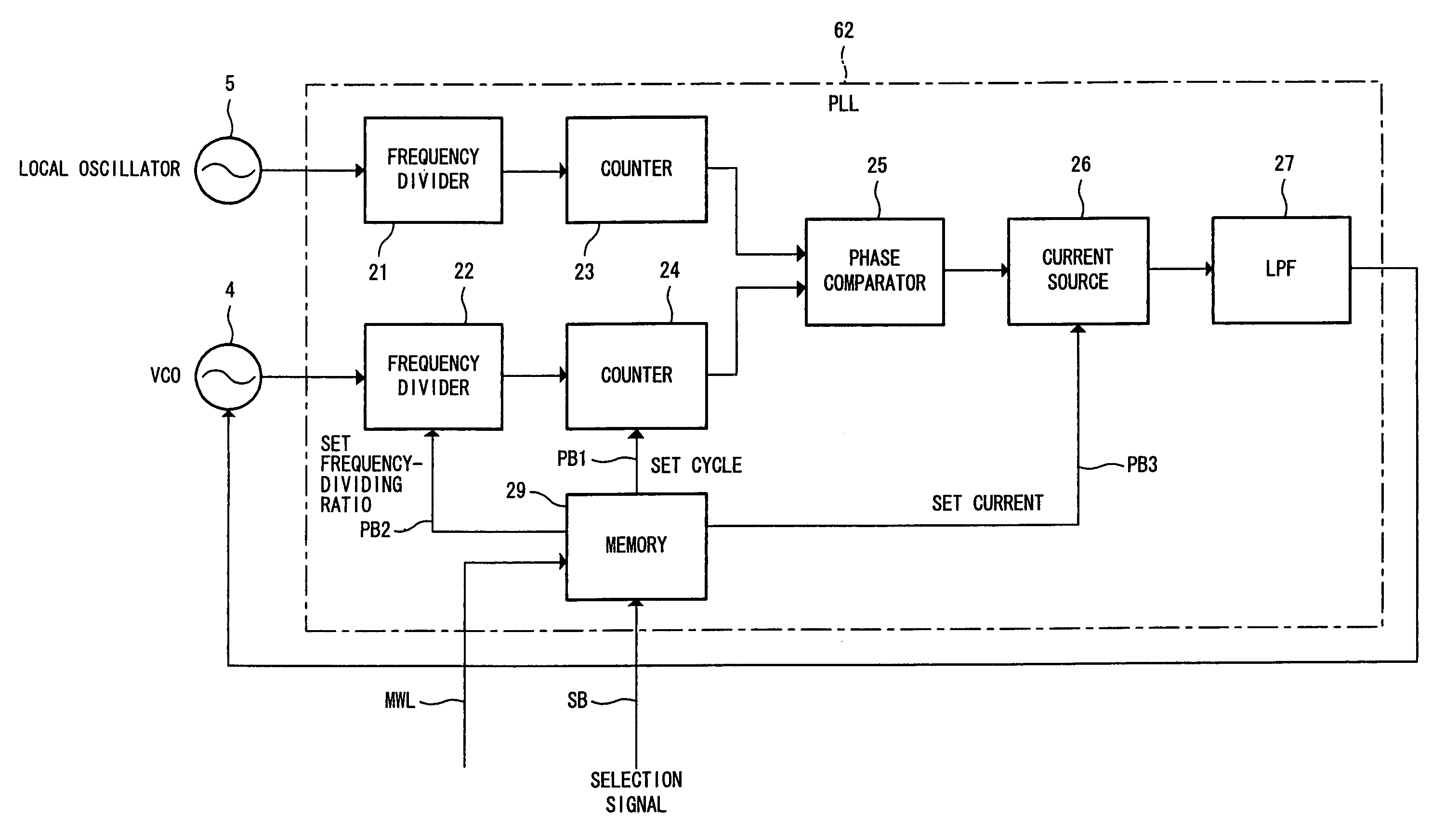
[0050]FIG. 3 is a block diagram illustrating an arrangement of a PLL circuit 62 according to the present embodiment.

[0051]As illustrated in FIG. 3, the PLL circuit 62, as with the PLL circuit 61 described above, has frequency dividers 21 and 22, counters 23 and 24, a phase comparator 25, a current source 26, a low-pass filter (LPF) 27. However, the PLL circuit 62 has a memory 29 instead of a memory 28.

[0052]Further, unlike the frequency divider 22 of the PLL circuit 61, the frequency divider 22 sets a frequency-dividing ratio and divides an output frequency of a VCO 4 at thus set frequency-dividing ratio. In case of changing a frequency accuracy in the PLL circuit 62, the frequency-dividing ratio setting of the frequency divider 22 is changed.

[0053]Moreover, unlike the current source 26 of the PLL circuit 61, the current source 26 selects and sets a plurality of current values (e.g., 2 mA and 4 mA) and outputs a current of a set current value. By changing a current value of the curr...

third embodiment

[0066]FIG. 5 is a block diagram illustrating an arrangement of a PLL circuit 63 according to the present embodiment.

[0067]As illustrated in FIG. 5, the PLL circuit 63, as with the PLL circuit 61, has frequency dividers 21 and 22, counters 23 and 24, a phase comparator 25, a current source 26, a low-pass filter (LPF) 27, a memory 29, and a selection circuit 30.

[0068]The selection circuit 30 selects, based on a selection signal supplied through a serial bus SB, either a setting pattern A inputted from outside through an external setting line ESL or a setting pattern B read out from the memory 29. The selection circuit 30 makes it possible to select a convenient set cycle depending on a situation. Such a situation is for example a situation where an external setting line ESL is used to operate the PLL circuit 63 at a value not stored in the memory 29 in the short run for testing and adjustment, and the memory 29 is used at normal times.

[0069]Further, the selection signal is transmitted...


PUM


Abstract

A PLL circuit has (i) a counter which divides a frequency of a VCO output whose frequency has been divided by a frequency divider and (ii) a memory which stores plural patterns of set cycles of the counter. The memory reads out one of the set cycles designated by a selection signal inputted through a serial bus (SB) from an outside of the PLL circuit. The set cycle, read out from the memory, which has a large amount of data, is inputted through a parallel bus (PB) into the counter, so that it hardly takes time to set a cycle for the counter. Further, even when the number of bits of the counter increases, the setting time is not lengthened.

Description

[0001]This Nonprovisional application claims priority under 35 U.S.C. § 119(a) on Patent Application No. 2004 / 177472 filed in Japan on Jun. 15, 2004, the entire contents of which are hereby incorporated by reference.FIELD OF THE INVENTION[0002]The present invention relates to a PLL (phase-locked loop) circuit included in a high-frequency receiving device which receives digital television broadcasting and the like.BACKGROUND OF THE INVENTION[0003]In digital television broadcasting, a high-frequency receiving device which demodulates a high-frequency signal into I and Q quadrature baseband signals is required in receiving a high-frequency signal (quadrature digital modulation signal) transmitted from a broadcasting station.[0004]FIG. 8 illustrates a general arrangement of a high-frequency receiving device 101 which demodulates a high-frequency signal into I and Q quadrature baseband signals.[0005]In the high-frequency receiving device 101, first, a high-frequency signal transmitted fr...

Claims


Application Information

Patent Timeline
Patent Type & Authority Patents(United States)
IPC IPC(8): H03D3/24G06F1/08H03L7/08H03L7/089H03L7/183H04B1/06H04B1/16H04B1/40H04B7/00
CPCH03L7/0898H03L7/183
Inventor YONEU, YUKI
Owner SHARP KK
Learn More