

Method of manufacturing a semiconductor apparatus
a manufacturing method and semiconductor technology, applied in the direction of semiconductor devices, semiconductor/solid-state device details, electrical devices, etc., can solve the problems of difficult roughening surface, high mounting density of semiconductor apparatuses, etc., and achieve high accuracy and improve mounting density.
- Summary
- Abstract
- Description
- Claims
- Application Information
AI Technical Summary
Benefits of technology
Problems solved by technology
Method used
Image

Examples
first embodiment
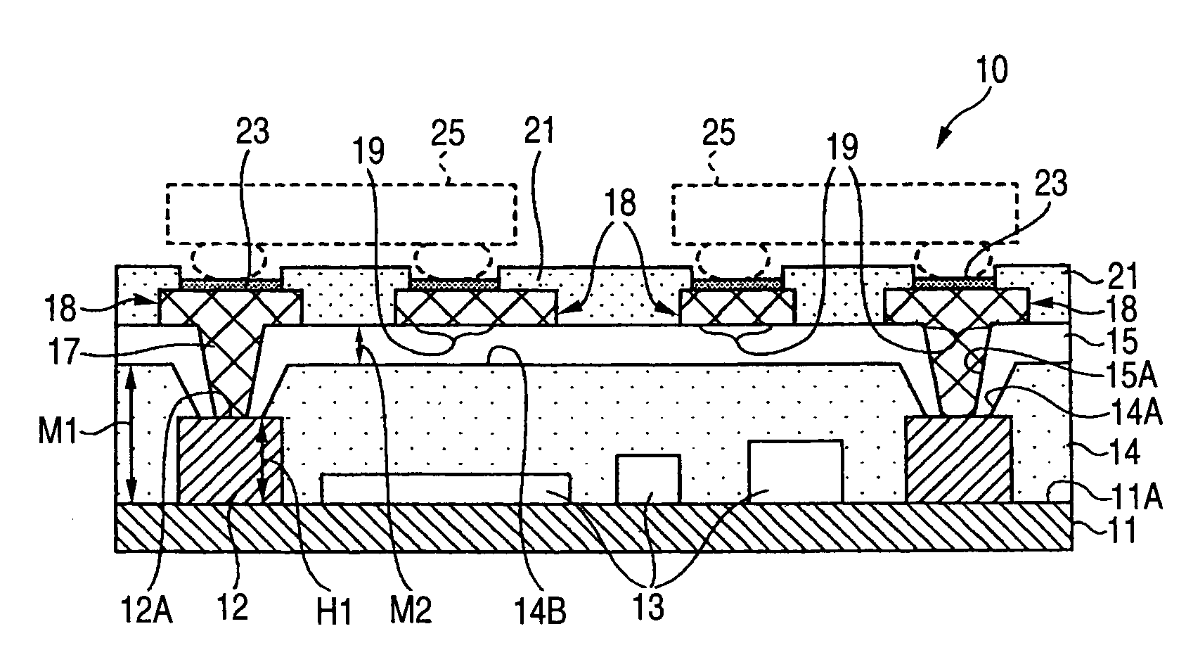
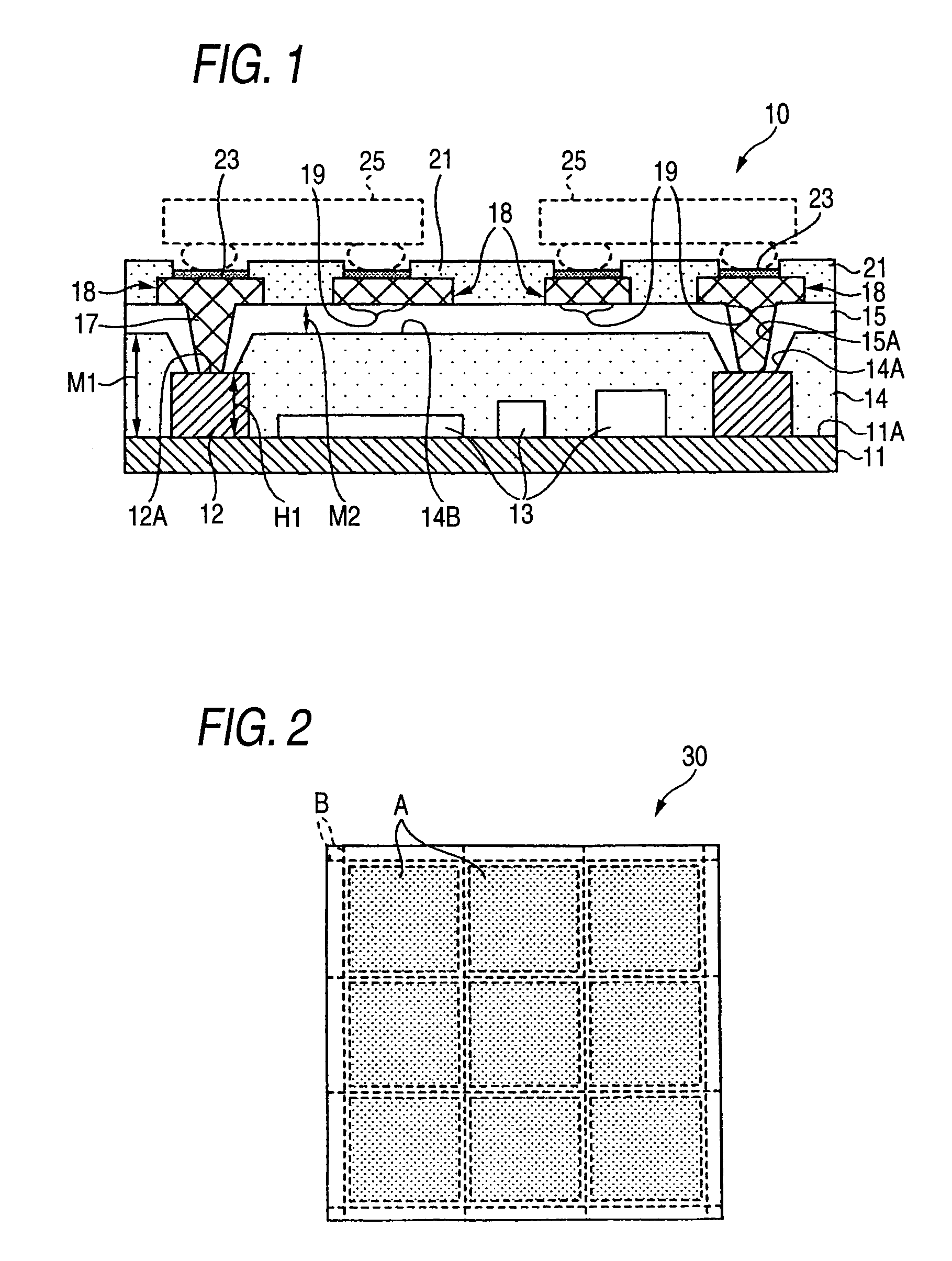
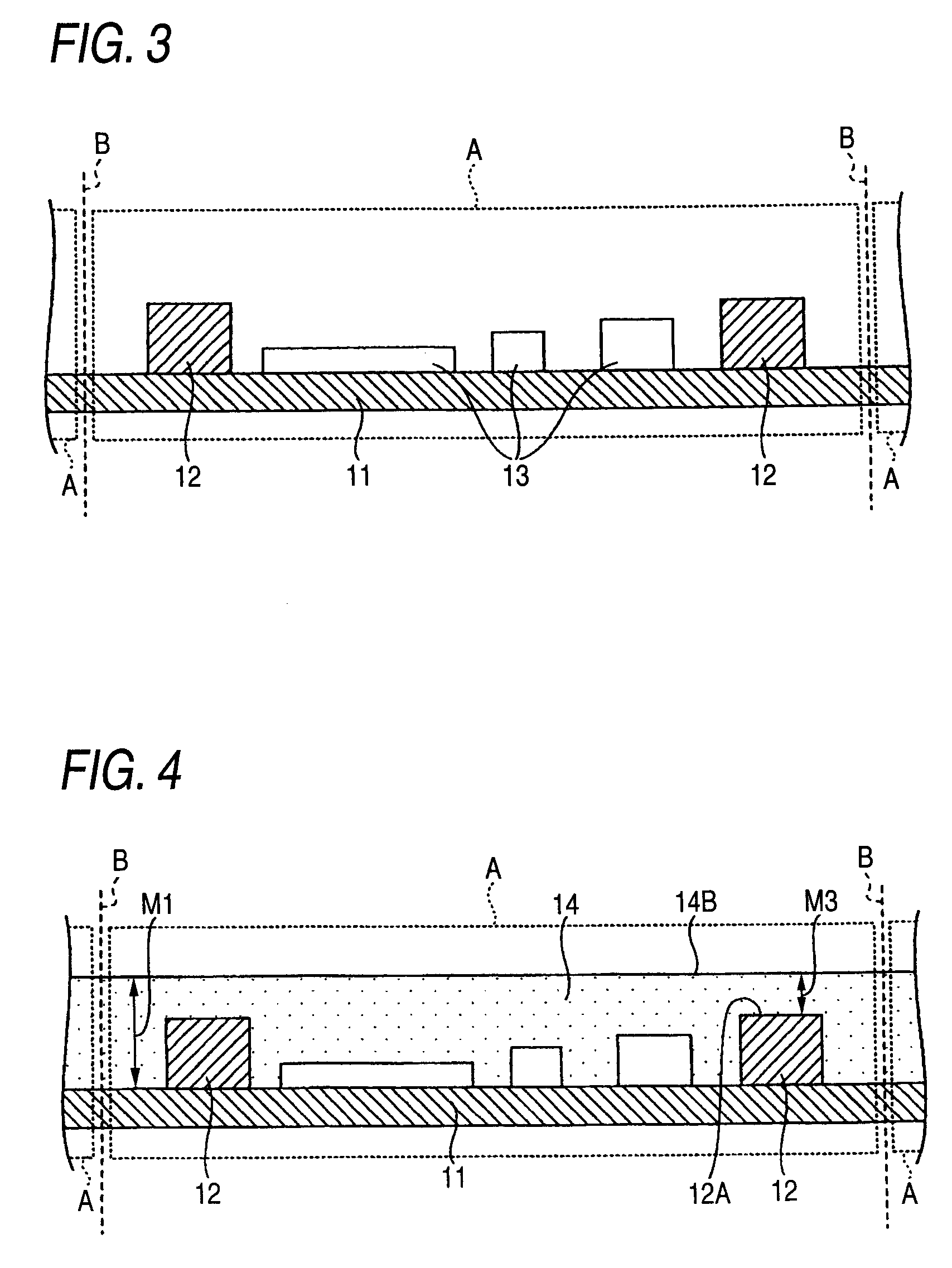
[0070]FIG. 1 is a sectional view of a semiconductor apparatus according to a first exemplary, non-limiting embodiment of the invention. In FIG. 1, H1 shows a height (hereinafter called “height H1”) of a terminal 12 for via connection, and M1 shows a thickness (hereinafter called “thickness M1”) of a sealing resin 14 in the case of using an upper surface 11A of a substrate 11 as the reference, and M2 shows a thickness (hereinafter called “thickness M2”) of a resin layer 15, respectively.
[0071]First, a semiconductor apparatus 10 according to the exemplary, non-limiting embodiment of the invention will be described with reference to FIG. 1. The semiconductor apparatus 10 has the substrate 11, the terminal 12 for via connection, electronic components 13, the sealing resin 14, the resin layer 15, a via 17, a wiring pattern 18, a protective film 21 and a diffusion preventive film 23.
[0072]The substrate 11 electrically connects the electronic components 13 to other substrates (not shown) s...
second embodiment
[0106]FIG. 17 is a sectional view of a semiconductor apparatus according to a second exemplary, non-limiting embodiment of the invention. In FIG. 17, M4 shows a thickness (hereinafter called “thickness M4”) of a sealing resin 41, and M5 shows a thickness (herein after called “thickness M5”) of a resin layer 42, respectively. Also, in FIG. 17, the same numerals are assigned to the same components as those of the semiconductor apparatus 10 of the first exemplary, non-limiting embodiment.
[0107]First, a semiconductor apparatus 40 according to the exemplary, non-limiting embodiment of the invention will be described with reference to FIG. 17. The semiconductor apparatus 40 has a configuration similar to that of the semiconductor apparatus 10 except that a sealing resin 41, a resin layer 42 and vias 45 are disposed instead of the sealing resin 14, the resin layer 15 and the vias 17 disposed in the semiconductor apparatus 10 of the first exemplary, non-limiting embodiment.
[0108]The sealing...
third embodiment
[0123]FIG. 23 is a sectional view of a semiconductor apparatus according to a third exemplary, non-limiting embodiment of the invention. In FIG. 23, M6 shows a thickness (hereinafter called “thickness M6”) of a resin layer 52, and M7 shows a thickness (hereinafter called “thickness M7”) of a shielding layer 53, respectively. Also, in FIG. 23, the same numerals are assigned to the same components as those of the semiconductor apparatus 10 of the first exemplary, non-limiting embodiment.
[0124]A semiconductor apparatus 50 according to the exemplary, non-limiting embodiment of the invention will be described with reference to FIG. 23. The semiconductor apparatus 50 has a substrate 11, electronic components 13, a sealing resin 14, a via 17, a ground terminal 51, the resin layer 52, the shielding layer 53 and a protective film 55.
[0125]The ground terminal 51 is a terminal set at a ground potential and is disposed on the substrate 11. The ground terminal 51 is electrically connected to the...
PUM
 Abstract
Description
Claims
Application Information