Optical transmission equipment and integrated circuit

a technology of optical transmission equipment and integrated circuit, which is applied in the direction of digital transmission, multi-channel communication, wavelength-division multiplex systems, etc., can solve the problems of delay adjustment, no practical solution in the documents 1 to 4 described above, and the transmission capacity has reached a limi

Inactive Publication Date: 2009-04-07
HITACHI LTD
View PDF5 Cites 15 Cited by
  • Summary
  • Abstract
  • Description
  • Claims
  • Application Information

AI Technical Summary

Benefits of technology

[0025]An object of the present invention is to provide optical transmission equipment that has effectively solved the problem of the delay difference among signal paths encountered when a sequence of transmission data are subjected to multilevel optical modulation using a plurality of optical modulators.
[0035]The control of the delay within the bit period can be implemented by, e.g., providing a clock generator for generating clock signals to be supplied to the multiplexing circuits and an accurate delay adjustment unit for adjusting the phase of a clock signal to be supplied to a specified one of the multiplexing circuits in accordance with a preliminarily specified amount of control and causing each of the multiplexing circuits to output each bit of the high-speed serial digital signal stream with a specified timing determined in accordance with the supplied clock signal. Since the delay control accuracy of the delay control buffer circuit can be improved to an integral fraction of the bit period by increasing the operating speed thereof, the adjustment of the delay within the bit period of the high-speed serial digital signal stream can be performed even in the absence of the accurate delay adjustment unit.
[0037]According to the present invention, the use of the delay control buffer circuits allows electric adjustment of a signal delay in each of the signal paths between an encoder for optical transmitter and an output optical fiber, with accuracy of the unit of bit length of the high-speed serial digital signal. As a result, even when a sequence of transmission data is divided into a plurality of digital signal streams and subjected to multilevel optical modulation via different signal paths, it becomes possible to make even the respective phases of the digital signal streams at the termination points of the signal paths. By increasing the operating speed of each of the delay control buffer circuits or by providing the accurate delay adjustment unit, precise adjustment of delay within the range of 1-bit-length of the high-speed serial digital signal stream can be realized.
[0038]According to the present invention, since the use of the delay control buffer circuits allows electric adjustment of a signal delay in the signal path between an input optical fiber and a decoder for optical receiver, a sequence of transmission data can easily be reproduced from a plurality of digital signal streams subjected to multilevel optical modulation.

Problems solved by technology

However, there is a feeling that the transmission capacity has reached a limit at about 10 Tbit / s (Terabit / second) and has continued to hover therearound for these several years.
However, none of Documents 1 to 4 described above has shown a practical solution to the problem associated with delay adjustment in individual signal paths that is encountered when transmission data (digital signal stream) is subjected to multilevel optical modulation using a plurality of optical modulators.
In the field of wireless communication to which the multilevel modulation is also applicable, there is no useful solution to the problem associated with delay adjustment in individual signal paths that is encountered in the optical transmission equipment described above.

Method used


Image

  • Optical transmission equipment and integrated circuit
  • Optical transmission equipment and integrated circuit
  • Optical transmission equipment and integrated circuit

Examples


embodiment 1

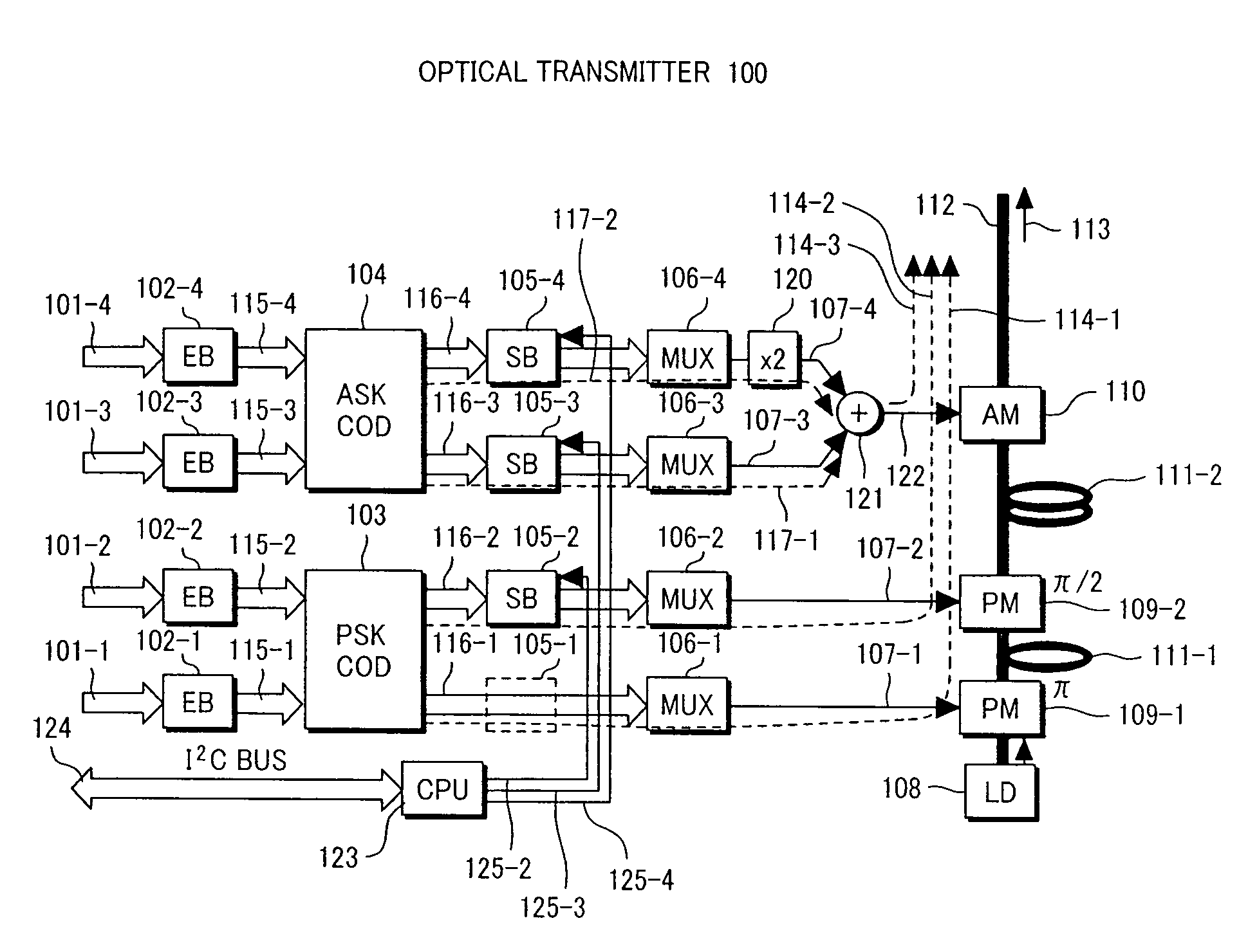
[0065]FIG. 1 shows a structure of an optical transmitter applied to optical transmission equipment according to a first embodiment of the present invention.

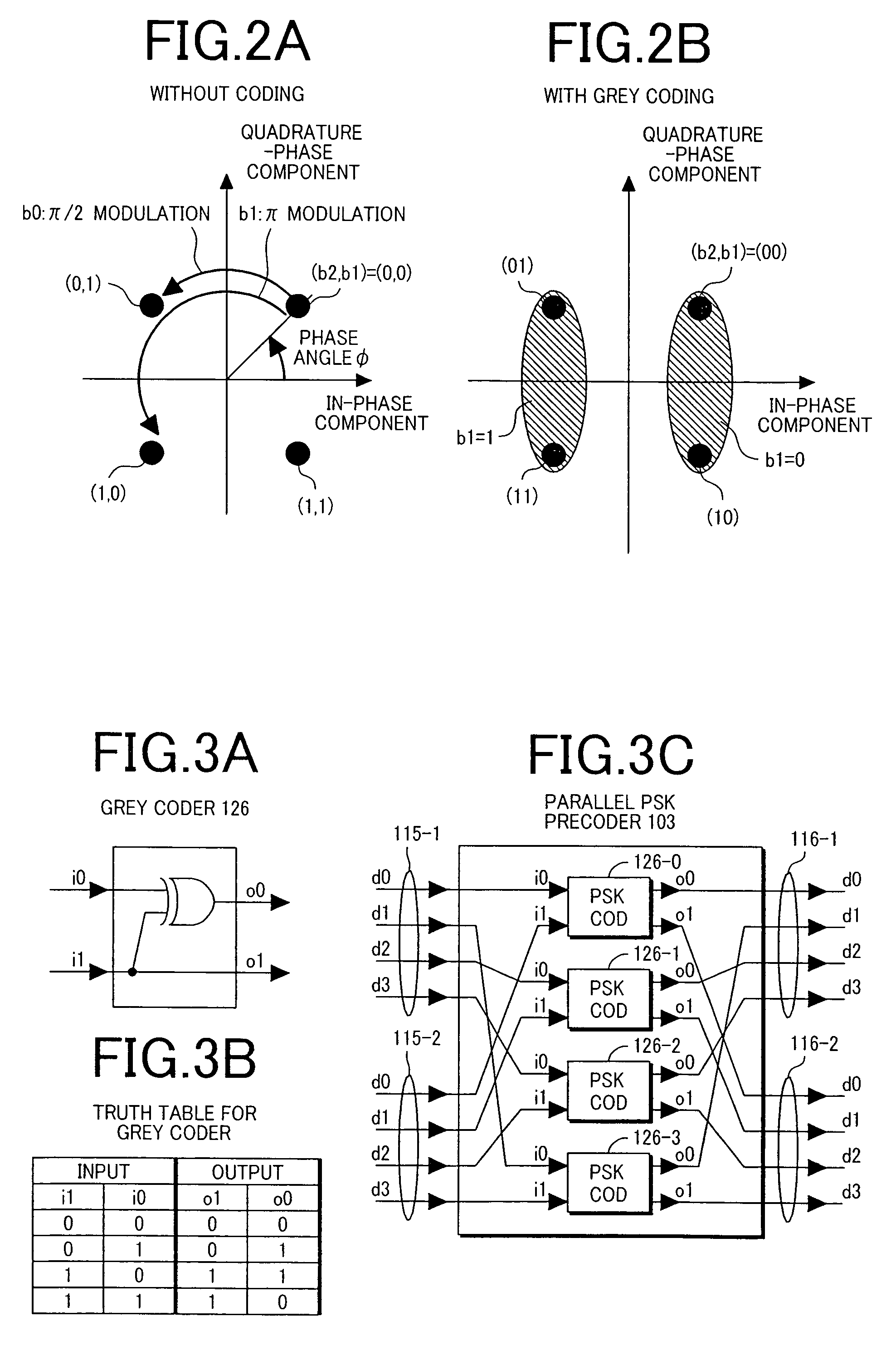
[0066]The optical transmitter 100 shown here comprises two encoders 103 and 104 using different encoding formats. The encoder 103 is a parallel precoder for four-level phase modulation (PSK precoder) and the encoder 104 is a parallel precoder for four-level intensity modulation (ASK precoder).

[0067]An optical modulation unit is comprised of two optical phase modulators 109-1 and 109-2, and one optical intensity modulator 110. An CW (continuous wave) optical signal generated from a semiconductor laser 108 is subjected to four-level phase modulation by the two optical phase modulators 109-1 and 109-2 associated with the PSK precoder 103 and four-level intensity modulation by the optical intensity modulator 110 associated with the ASK precoder 104 and sent out as a 16-level optical phase / intensity modulated signal 113 to an output o...

embodiment 2

[0145]FIG. 11 shows an example of an optical network to which optical transmission equipment 160 according to the present invention have been applied.

[0146]Optical transmission equipment 160-1 comprises a plurality of optical transmitters 100 (100-1 and 100-2) and optical receivers 200 (200-1 and 200-2) connected to a switch circuit 162-1. Likewise, optical transmission equipment 160-2 also comprises a plurality of optical transmitters 100 (100-3 and 100-4) and optical receivers 200 (200-3 and 200-4) connected to a switch circuit 162-2. The optical transmitter 100-1 and the optical receiver 200-3, which are in mutually opposing positional relation, and the optical transmitter 100-4 and the optical receiver 200-2, which are also in mutually opposing positional relation, are connected to each other via optical fiber transmission paths 164-1 and 162-2, respectively.

[0147]Each of the optical transmission equipment 160 is capable of switching between a working system and a standby system...

embodiment 3

[0153]FIG. 13 shows an example of an optical network comprised of WDM type optical transmission equipment 165 (165-1 and 165-2) to which the present invention has been applied.

[0154]The optical transmission equipment 165-1 and 165-2 are coupled to each other through an upward optical fiber transmission path 164-1 and a downward optical fiber transmission path 164-2. The optical transmission equipment is further connected to other optical transmission equipment by a pair of upward and downward optical fiber transmission paths, as shown by the optical fiber transmission paths 164-3 and 164-4 in the drawing. Each of the optical fibers transmits three optical signals at different wavelengths as wavelength multiplexed optical signals.

[0155]As shown in the optical transmission equipment 165-1, each of the optical transmission equipment 165 comprises a plurality of optical receivers (RX) 200 (200-1 to 200-3 and 200-4 to 200-6) each coupled to the receiving-side optical fiber transmission p...


PUM


Abstract

Optical transmission equipment, capable of electrically adjusting the delay difference between a plurality of digital signal paths to be connected to a multilevel optical modulation unit or demodulation unit, having multiplexing circuits connected to the digital signal paths and a delay adjustment unit inserted in one of the digital signal paths to adjust delay of N-bit-parallel low-speed digital signals with the timing unit of a bit period of a high-speed serial digital signal to be outputted from multiplexing circuit.

Description

CLAIM OF PRIORITY[0001]The present application claims priority from Japanese application serial No. 2005-158926, filed on May 31, 2005, the content of which is hereby incorporated by reference into this application.BACKGROUND OF THE INVENTION[0002](1) Field of the Invention[0003]The present invention relates to optical transmission equipment and to an integrated circuit. More particularly, the present invention relates to optical transmission equipment comprising an optical modulation unit including a plurality of optical modulators or an optical demodulation unit for receiving a multilevel modulated optical signal from an external optical transmission line and outputting a plurality of electric high-speed serial digital signal streams converted from the received signal and to an integrated circuit applicable to the optical transmission equipment.[0004](2) Description of Related Art[0005]The recent increases in the number of wavelengths in WDM transmission and in optical signal modu...

Claims


Application Information

Patent Timeline
Patent Type & Authority Patents(United States)
IPC IPC(8): H04B10/00H04B10/40H04B10/07H04B10/50H04B10/516H04B10/524H04B10/54H04B10/556H04B10/60H04B10/61H04B10/67H04B10/69H04J14/00H04J14/02H04L27/34
CPCH04B10/152H04B10/505H04B10/5051H04B10/5053H04B10/5055H04B10/5161H04B10/541H04B10/5561H04B10/66H04L27/2096H04L27/223
Inventor KIKUCHI, NOBUHIKO
Owner HITACHI LTD
Why Eureka
Try Eureka