
Dicing/die bonding sheet

a technology of die bonding and die bonding, which is applied in the direction of heat-activated film/foil adhesives, film/foil adhesives, synthetic resin layered products, etc., can solve the problems that film adhesives and dicing tapes may not separate satisfactorily, and achieve satisfactory adhesiveness.

Active Publication Date: 2009-04-14
RESONAC CORPORATION +1
View PDF12 Cites 24 Cited by
  • Summary
  • Abstract
  • Description
  • Claims
  • Application Information

AI Technical Summary

Benefits of technology

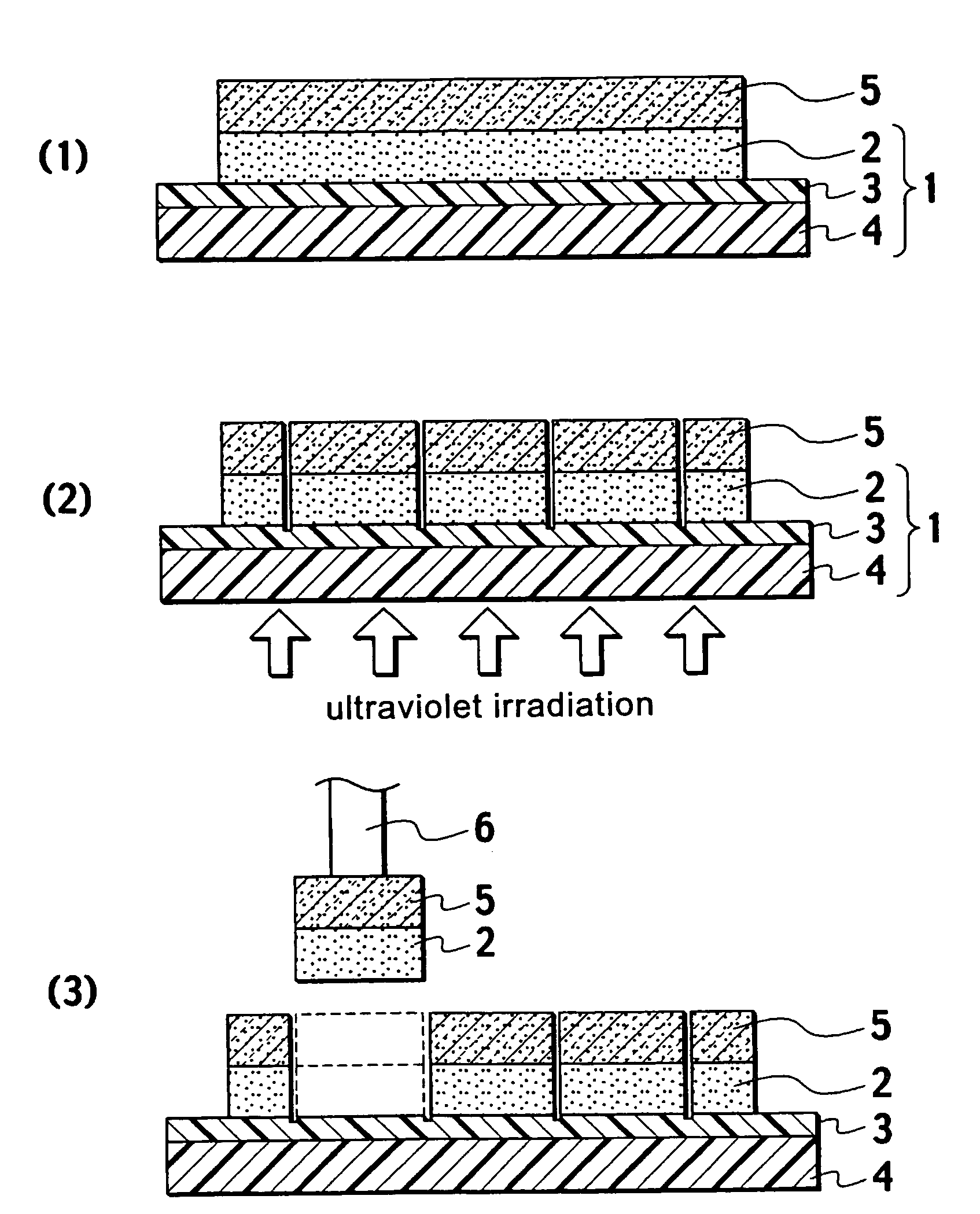
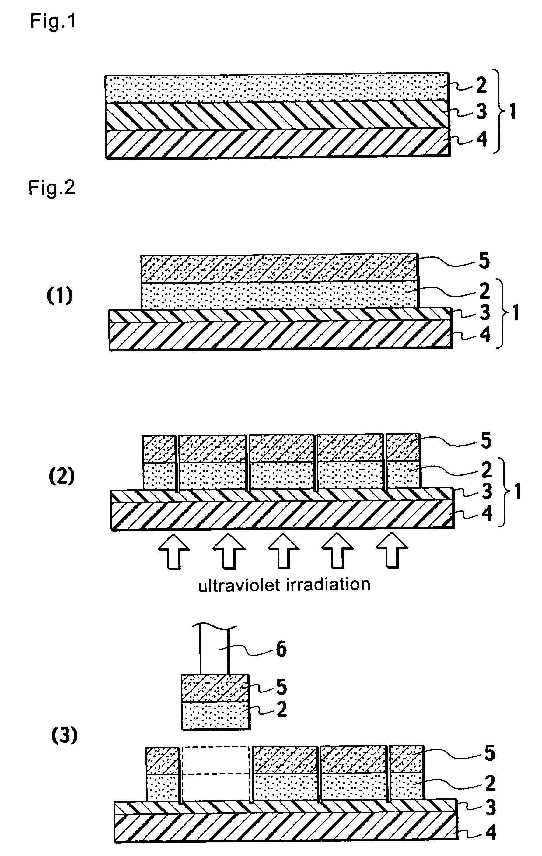
[0008]Accordingly, an object of the present invention is to provide a dicing / die bonding sheet which can be laminated to a semiconductor wafer and used as a dicing tape during dicing, enables ready separation of the semiconductor element and the adhesive layer from the pressure-sensitive adhesive layer during pickup, and in which the adhesive layer has satisfactory adhesiveness as a die bonding material.

Problems solved by technology

However, with an integrated dicing / die bonding sheet comprising a film adhesive provided on a dicing tape, because the period between manufacture and use of the sheet, during which time the adhesive layer of the film adhesive is in contact with the pressure-sensitive adhesive layer of the dicing sheet, is inevitably long, a problem arises in that the two layers interact, meaning that during the process for picking up individual semiconductor elements with the film adhesive laminated thereto, the film adhesive and the dicing tape may not separate satisfactorily.

Method used


Image

  • Dicing/die bonding sheet
  • Dicing/die bonding sheet
  • Dicing/die bonding sheet

Examples


examples

[0096]As follows is a more detailed description of the present invention based on a series of examples, although the present invention is in no way limited by the examples presented below.

[0097]Radiation curable pressure-sensitive adhesives were prepared as described below in examples 1 to 6 and comparative examples 1 to 3, and were each then applied to an ethylene-vinyl acetate copolymer film in the manner described below, thus forming an adhesive tape. Subsequently, an adhesive film prepared in advance in the manner described below was laminated to the pressure-sensitive adhesive layer of the adhesive tape, yielding a dicing / die bonding sheet.

[0098]The properties of the dicing / die bonding sheets prepared in this manner were tested and evaluated. These properties were evaluated in the following manner.

1) Peel Strength

[0099]This is an indicator of the ease with which the laminated adhesive film and adhesive tape are able to be peeled apart. Prior to ultraviolet irradiation, in order...

examples 1 to 6

[0112]Samples of the adhesive film 1 were laminated to the adhesive tapes described above to prepare the dicing / die bonding sheets of the examples 1 to 6 and the comparative examples 1 to 3 shown in Table 1, and the properties of these sheets were then evaluated.

[0113]As shown in the examples 1 through 6, with the dicing / die bonding sheets prepared by laminating the adhesive film 1 to an adhesive tape produced using one of the pressure-sensitive adhesive compositions 1 to 6, irradiation following dicing causes a satisfactory reduction in the peel strength of the pressure-sensitive adhesive layer, meaning during pickup, the structure separates between the pressure-sensitive adhesive layer and the adhesive layer, resulting in a favorable pickup success rate. Furthermore, with these dicing / die bonding sheets, even if the entire dicing / die bonding sheet is irradiated following dicing, a satisfactory spacing can still be retained between elements when the dicing / die bonding sheet is subj...


PUM

PropertyMeasurementUnit
glass transition temperatureaaaaaaaaaa
particle diameteraaaaaaaaaa
heat resistanceaaaaaaaaaa

Abstract

The present invention provides a dicing / die bonding sheet which can be used as a dicing tape during dicing, enables ready separation of the semiconductor element and the adhesive layer from the pressure-sensitive adhesive layer during pickup, and in which the adhesive layer has satisfactory adhesiveness as a die bonding material. A dicing / die bonding sheet in which the pressure-sensitive adhesive layer comprises a compound (A), containing intramolecular, radiation curable carbon-carbon double bonds with an iodine value of 0.5 to 20, and at least one compound (B) selected from a group consisting of polyisocyanates, melamine-formaldehyde resins, and epoxy resins, and the adhesive layer comprises an epoxy resin (a), a phenolic resin (b) with a hydroxyl equivalent of at least 150 g / eq., an epoxy group-containing acrylic copolymer (c), comprising from 0.5 to 6% by weight of glycidyl acrylate or glycidyl methacrylate, and with a weight average molecular weight of at least 100,000, a filler (d), and a curing accelerator (e).

Description

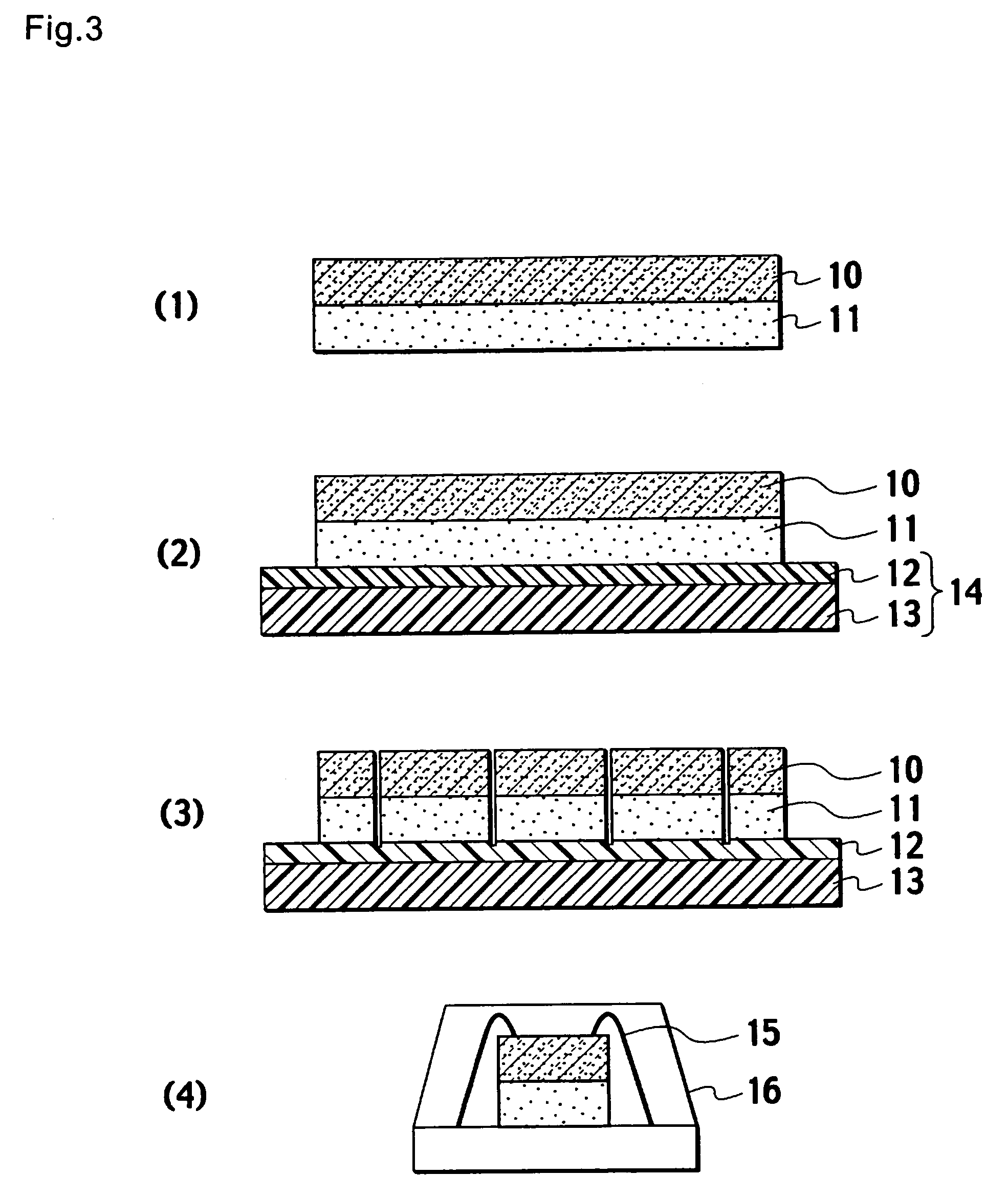
TECHNICAL FIELD[0001]The present invention relates to a dicing / die bonding sheet used in both a dicing process, in which a semiconductor wafer is cut and separated into semiconductor elements, and a die bonding process, in which the semiconductor elements are bonded to support members.BACKGROUND ART[0002]In recent years, wafer backside laminating methods have been widely used as a process for cutting and separating (dicing) semiconductor wafers that have been produced with a large diameter into smaller semiconductor elements (semiconductor chips), and then bonding (die bonding) each of these semiconductor elements onto a support member such as a lead frame or an organic substrate.[0003]When a semiconductor device is manufactured by a wafer backside laminating method, using a film adhesive, then as shown in FIG. 3, first, (1) a film adhesive 11 is laminated to the backside of a semiconductor wafer 10, and then (2) a dicing tape 14, comprising a pressure-sensitive adhesive layer 12 di...

Claims


Application Information

Patent Timeline
Patent Type & Authority Patents(United States)
IPC IPC(8): H01L21/00C08L63/00C09J7/35C09J133/06C09J133/14C09J157/00C09J161/06C09J161/10C09J161/28C09J163/00C09J163/10C09J175/04C09J175/14H01L21/78
CPCC09J133/068C09J161/06C09J161/28C09J163/10C09J175/14C09J7/0203H01L24/83H01L24/29H01L24/27C08L63/00H01L2224/83191C09J2201/36C09J2201/606C09J2203/326C09J2461/00C09J2463/00C09J2475/00H01L2224/73265C08L2666/02C08L2666/22C09J7/35C09J2301/208C09J2301/302B32B27/08H01L21/70
Inventor HATAKEYAMA, KEIICHIURUNO, MICHIOMATSUZAKI, TAKAYUKIMORISHIMA, YASUMASAKITA, KENJIISHIWATA, SHINICHI
Owner RESONAC CORPORATION
Learn More